Maximum ratings, Thermal characteristics, Electrical characteristics – Diodes DMP2004K User Manual
Page 2: Dmp2004k
DMP2004K
Document number: DS30933 Rev. 7 - 2
2 of 5
July 2012
© Diodes Incorporated
DMP2004K
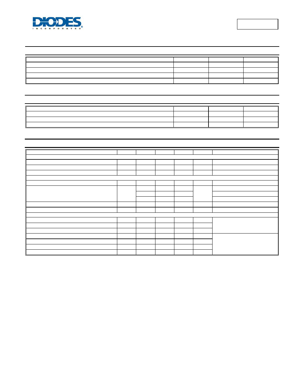
Maximum Ratings
(@T
A
= +25°C, unless otherwise specified.)
Characteristic Symbol
Value
Units
Drain-Source Voltage
V
DSS
-20 V
Gate-Source Voltage
V
GSS
±8 V
Continuous Drain Current (Note 5) V
GS
= -4.5V
I
D
-600 mA
Pulsed Drain Current
I
DM
-1.9 A
Thermal Characteristics
Characteristic Symbol
Value
Units
Total Power Dissipation (Note 5)
P
D
550 mW
Thermal Resistance, Junction to Ambient (Note 5)
R
θJA
227 °C/W
Operating and Storage Temperature Range
T
J,
T
STG
-55 to +150
°C
Electrical Characteristics
(@T
A
= +25°C, unless otherwise specified.)
Characteristic Symbol
Min
Typ
Max
Unit
Test
Condition
OFF CHARACTERISTICS (Note 6)
Drain-Source Breakdown Voltage
BV
DSS
-20 — — V
V
GS
= 0V, I
D
= -250µA
Zero Gate Voltage Drain Current
I
DSS
— — -1 µ
A
V
DS
= -20V, V
GS
= 0V
Gate-Source Leakage
I
GSS
— —
±1.0
µA
V
GS
= ±4.5V, V
DS
= 0V
ON CHARACTERISTICS (Note 6)
Gate Threshold Voltage
V
GS(th)
-0.5 — -1.0 V
V
DS
= V
GS
, I
D
= -250µA
Static Drain-Source On-Resistance
R
DS (ON)
— 0.7 0.9
Ω
V
GS
= -4.5V, I
D
= -430mA
— 1.1 1.4
V
GS
= -2.5V, I
D
= -300mA
— 1,7 2.0
V
GS
= -1.8V, I
D
= -150mA
Forward Transfer Admittance
|Y
fs
|
200 — — mS
V
DS
= -10V, I
D
= -0.2A
Diode Forward Voltage (Note 6)
V
SD
-0.5 — -1.2 V
V
GS
= 0V, I
S
= -115mA
DYNAMIC CHARACTERISTICS (Note 7)
Input Capacitance
C
iss
— — 175 pF
V
DS
= -16V, V
GS
= 0V
f = 1.0MHz
Output Capacitance
C
oss
— — 30 pF
Reverse Transfer Capacitance
C
rss
— — 20 pF
Turn-On Delay Time
t
D(on)
— 8.5 — ns
V
DD
= -3V, V
GS
= -2.5V,
R
L
= 300
Ω, R
G
= 25
Ω,
I
D
= -100mA
Turn-On Rise Time
t
r
— 4.3 — ns
Turn-Off Delay Time
t
D(off)
— 20.2 — ns
Turn-Off Fall Time
t
f
— 19.2 — ns
Notes:
5. Device mounted on FR-4 PCB.
6. Short duration pulse test used to minimize self-heating effect.
7. Guaranteed by design. Not subject to product testing.