Maximum ratings, Thermal characteristics – Diodes DMN6066SSS User Manual
Page 2
DMN6066SSS
Document Number DS32110 Rev 2 - 2
2 of 9
November 2011
© Diodes Incorporated
A Product Line of
Diodes Incorporated
DMN6066SSS
ADVAN
CE I
N
F
O
RM
ATI
O
N
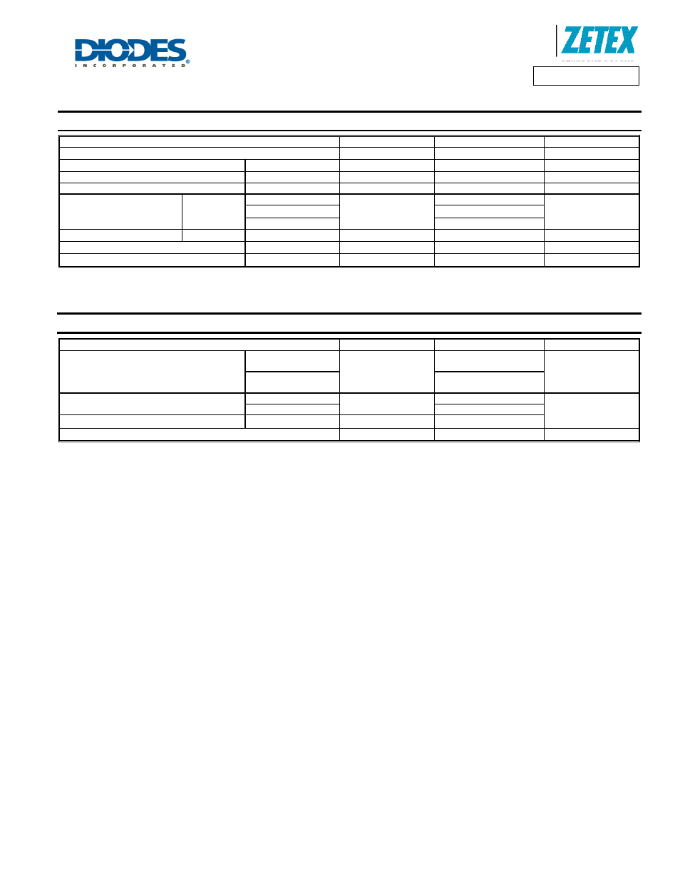
Maximum Ratings
@T
A
= 25°C unless otherwise specified
Characteristic Symbol
Value
Unit
Drain-Source voltage
V
DSS
60 V
Gate-Source voltage
(Note 2)
V
GS
±20
V
Single Pulsed Avalanche Energy
(Note 7)
E
AS
37.5 mJ
Single Pulsed Avalanche Current
(Note 7)
I
AS
5.0 A
Continuous Drain current
V
GS
= 10V
(Note 4)
I
D
5.0
A
T
A
= 70°C (Note 4)
4.0
(Note 3)
3.7
Pulsed Drain current
V
GS
= 10V
(Note 5)
I
DM
23 A
Continuous Source current (Body diode)
(Note 4)
I
S
4.0 A
Pulsed Source current (Body diode)
(Note 5)
I
SM
23 A
Thermal Characteristics
@T
A
= 25°C unless otherwise specified
Characteristic Symbol
Value
Unit
Power dissipation
Linear derating factor
(Note 3)
P
D
1.56
12.5
W
mW/
°C
(Note 4)
2.81
22.5
Thermal Resistance, Junction to Ambient
(Note 3)
R
θJA
80.0
°C/W
(Note 4)
44.5
Thermal Resistance, Junction to Lead
(Note 6)
R
θJL
37.0
Operating and storage temperature range
T
J
, T
STG
-55 to 150
°C
Notes:
2. AEC-Q101 V
GS
maximum is
±16V.
3. For a device surface mounted on 25mm x 25mm x 1.6mm FR4 PCB with high coverage of single sided 1oz copper, in still air conditions; the device is
measured when operating in a steady-state condition.
4. Same as note (3), except the device is measured at t
≤ 10 sec.
5. Same as note (3), except the device is pulsed with D= 0.02 and pulse width 300 µs. The pulse current is limited by the maximum junction temperature.
6. Thermal resistance from junction to solder-point (at the end of the drain lead).
7. UIS in production with L = 3.0mH, I
AS
= 5.0A, R
G
= 25
Ω, V
DD
=50V, starting T
J
= 25°C.