Electrical characteristics - mosfet, Electrical characteristics - npn transistor, Dmb53d0udw – Diodes DMB53D0UDW User Manual
Page 2
DMB53D0UDW
Document number: DS31675 Rev. 5 - 2
2 of 7
December 2009
© Diodes Incorporated
DMB53D0UDW
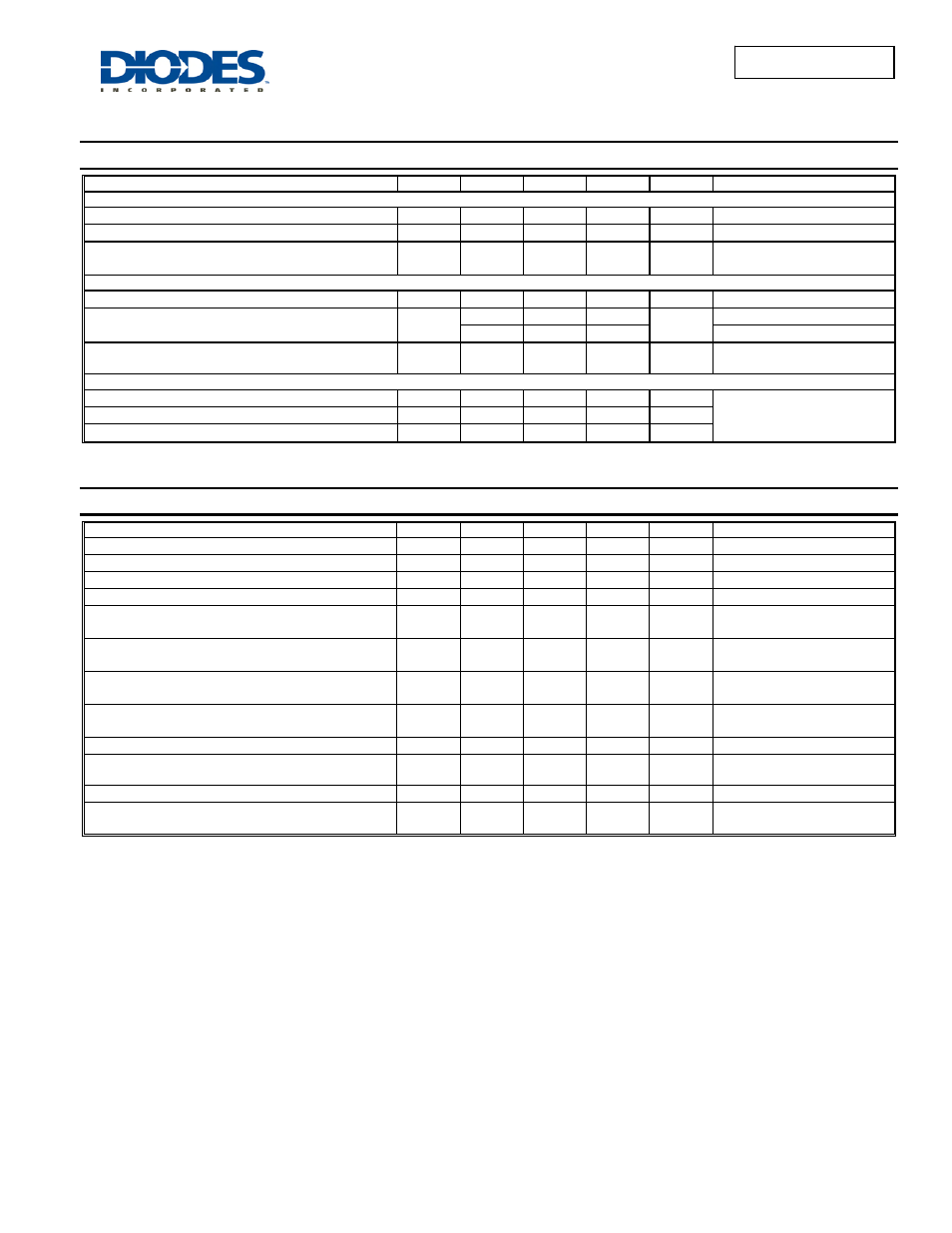
Electrical Characteristics - MOSFET
@T
A
= 25°C unless otherwise specified
Characteristic Symbol
Min
Typ
Max
Unit
Test
Condition
OFF CHARACTERISTICS (Note 2)
Drain-Source Breakdown Voltage
BV
DSS
50
⎯
⎯
V
V
GS
= 0V, I
D
= 250
μA
Zero Gate Voltage Drain Current
I
DSS
⎯
⎯
10
μA
V
DS
= 50V, V
GS
= 0V
Gate-Body Leakage
I
GSS
⎯
⎯
1.0
5.0
μA
V
GS
=
±8V, V
DS
= 0V
V
GS
=
±12V, V
DS
= 0V
ON CHARACTERISTICS (Note 2)
Gate Threshold Voltage
V
GS(th)
0.7 0.8 1.0 V
V
DS
= V
GS
, I
D
= 250
μA
Static Drain-Source On-Resistance
R
DS (ON)
⎯
3.1 4 Ω
V
GS
= 4V, I
D
= 100mA
⎯
4 5
V
GS
= 2.5V, I
D
= 80mA
Forward Transconductance
g
FS
180
⎯
⎯
mS
V
DS
= 10V, I
D
= 100mA,
f = 1.0KHz
DYNAMIC CHARACTERISTICS
Input Capacitance
C
iss
⎯
25
⎯
pF
V
DS
= 10V, V
GS
= 0V,
f = 1.0MHz
Output Capacitance
C
oss
⎯
5
⎯
pF
Reverse Transfer Capacitance
C
rss
⎯
2.1
⎯
pF
Electrical Characteristics - NPN Transistor
@T
A
= 25°C unless otherwise specified
Characteristic Symbol
Min
Typ
Max
Unit
Test
Condition
Collector-Base Breakdown Voltage (Note 4)
V
(BR)CBO
50 — — V
I
C
= 10
μA, I
B
= 0
Collector-Emitter Breakdown Voltage (Note 4)
V
(BR)CEO
45 — — V
I
C
= 10mA, I
B
= 0
Emitter-Base Breakdown Voltage (Note 4)
V
(BR)EBO
6 — — V
I
E
= 1
μA, I
C
= 0
DC Current Gain (Note 4)
h
FE
200 290 450 —
V
CE
= 5.0V, I
C
= 2.0mA
Collector-Emitter Saturation Voltage (Note 4)
V
CE(SAT)
— —
100
300
mV
I
C
= 10mA, I
B
= 0.5mA
I
C
= 100mA, I
B
= 5.0mA
Base-Emitter Saturation Voltage (Note 4)
V
BE(SAT)
—
700
900
— mV
I
C
= 10mA, I
B
= 0.5mA
I
C
= 100mA, I
B
= 5.0mA
Base-Emitter Voltage (Note 4)
V
BE
580
—
660
—
700
770
mV
V
CE
= 5.0V, I
C
= 2.0mA
V
CE
= 5.0V, I
C
= 10mA
Collector Cut-Off Current
(Note 4)
I
CBO
— —
15
5.0
nA
µA
V
CB
= 30V
V
CB
= 30V, T
A
= 150°C
Collector-Emitter Cut-Off Current
(Note 4)
I
CES
— — 100 nA
V
CE
= 45V
Gain Bandwidth Product
f
T
100 — — MHz
V
CE
= 5.0V, I
C
= 10mA,
f = 100MHz
Output Capacitance
C
OBO
— — 4.5 pF
V
CB
= 10V, f = 1.0MHz
Noise Figure
NF
—
—
10
dB
V
CE
= 5V, R
S
= 2.0k
Ω,
f = 1.0kHz, BW
= 200Hz
Notes:
4. Short duration pulse test used to minimize self-heating effect.