Maximum ratings, Thermal characteristics, Dmn3730u – Diodes DMN3730U User Manual
Page 2: A product line of diodes incorporated
DMN3730U
Datasheet number: DS35308 Rev. 2 - 2
2 of 7
July 2011
© Diodes Incorporated
DMN3730U
A Product Line of
Diodes Incorporated
Maximum Ratings
@T
A
= 25°C unless otherwise specified
Characteristic
Symbol
Value
Unit
Drain-Source Voltage
V
DSS
30 V
Gate-Source Voltage
V
GSS
±8 V
Continuous Drain Current
Steady
State
T
A
= 25°C (Note 5)
T
A
= 85°C (Note 5)
T
A
= 25°C (Note 4)
I
D
0.94
0.68
0.75
A
Pulsed Drain Current (Note 6)
I
DM
10 A
Thermal Characteristics
@T
A
= 25°C unless otherwise specified
Characteristic Symbol
Value
Unit
Power Dissipation
(Note 4)
P
D
0.45 W
(Note 5)
0.71
W
Thermal Resistance, Junction to Ambient
(Note 4)
R
θJA
275 °C/W
(Note 5)
177
°C/W
Operating and Storage Temperature Range
T
J
,
T
STG
-55 to +150
°C
Notes:
4. Device mounted on FR-4 substrate PC board, 2oz copper, with minimum recommended pad layout
5. Device mounted on 25mm X 25mm square copper plate with FR-4 substrate PC board, 2oz copper
6. Device mounted on minimum recommended pad layout test board, 10
μ
s pulse duty cycle = 1%.
Thermal Characteristics
0.001
0.01
0.1
1
10
100
1000
T1, PULSE DURATION SECTION (sec)
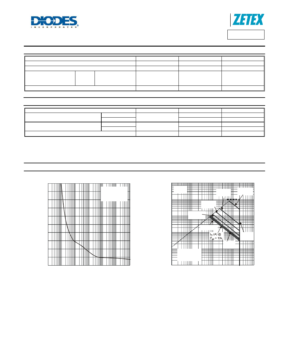
Fig. 1 Single Maximum Power Dissipation
0
10
20
30
40
50
60
70
80
90
100
P
(p
k
),
P
EA
K
T
R
ANS
IE
N
T
P
O
WE
R
(W
)
Single Pulse
Rthja = 176C/W
Rthja(t) = Rthja*r(t)
T - T = P*Rthja (t)
J
A
0.01
0.1
1
10
100
V
, DRAIN-SOURCE VOLTAGE
Fig. 2 SOA, Safe Operation Area
DS
100
0.001
0.01
0.1
1
10
I,
D
R
AI
N
C
U
R
R
E
N
T
(A
)
D
I (A) @
P = 1s
D
W
I (A) @
P = 1ms
D
W
I (A) @
P = 100µs
D
W
I (A) @
P = 10µs
D
W
I (A) @ DC
D
I (A) @
P = 100ms
D
W
I (A) @
P = 10ms
D
W
R
Limited
DS(ON)
T , (Max) = 150°C
T = 25°C
Single Pulse
J
A