Diodes DMN32D2LDF User Manual
Dmn32d2ldf, Features, Mechanical data
DMN32D2LDF
COMMON SOURCE DUAL N-CHANNEL
ENHANCEMENT MODE FIELD EFFECT TRANSISTOR
Features
•
Common Source Dual N-Channel MOSFET
•
Low On-Resistance
•
Very Low Gate Threshold Voltage, 1.2V max
•
Low Input Capacitance
•
Fast Switching Speed
•
Low Input/Output Leakage
•
Small Surface Mount Package
•
ESD Protected Gate
•
Lead Free By Design/RoHS Compliant (Note 2)
•
"Green" Device (Note 3)
•
Qualified to AEC-Q 101 Standards for High Reliability
Mechanical Data
•
Case: SOT-353
•
Case Material: Molded Plastic, “Green” Molding
Compound. UL Flammability Classification Rating 94V-0
•
Moisture Sensitivity: Level 1 per J-STD-020C
•
Terminal Connections: See Diagram
•
Terminals: Finish – Matte Tin annealed over Alloy 42
leadframe. Solderable per MIL-STD-202, Method 208
•
Marking Information: See Page 3
•
Ordering Information: See Page 3
•
Weight: 0.006 grams (approximate)
NEW PRODUCT
G
1
D
1
G
2
D
2
S
Q
1
Q
2
G
2
S
G
1
D
2
D
1
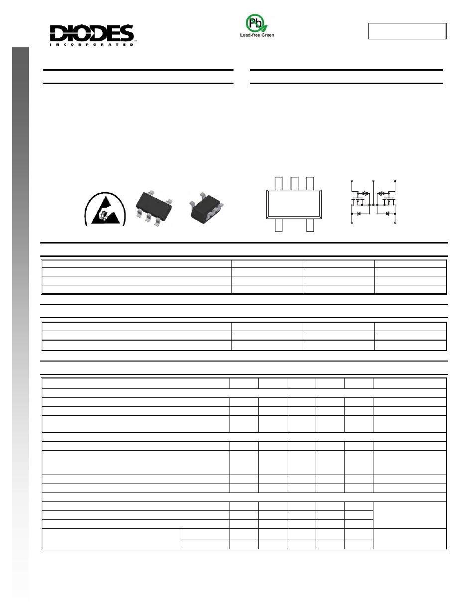
SOT-353
ESD PROTECTED
TOP VIEW
BOTTOM VIEW
Schematic Diagram
TOP VIEW
Maximum Ratings Q
1
, Q
2
@T
A
= 25°C unless otherwise specified
Characteristic Symbol
Value
Unit
Drain Source Voltage
V
DSS
30 V
Gate-Source Voltage
V
GSS
±10
V
Drain Current (Note 1)
I
D
400 mA
Thermal Characteristics
Q
1
, Q
2
@T
A
= 25°C unless otherwise specified
Total Power Dissipation (Note 1)
P
D
280 mW
Thermal Resistance, Junction to Ambient (Note 1)
R
θJA
446
°C/W
Operating and Storage Temperature Range
T
j
, T
STG
-55 to +150
°C
Electrical Characteristics Q
1
, Q
2
@T
A
= 25°C unless otherwise specified
Characteristic Symbol
Min
Typ
Max
Unit
Test
Condition
OFF CHARACTERISTICS (Note 4)
Drain-Source Breakdown Voltage
BV
DSS
30
⎯
⎯
V
V
GS
= 0V, I
D
= 250
μA
Zero Gate Voltage Drain Current
@ T
C
= 25°C
I
DSS
⎯
⎯
1
μA
V
DS
= 30V, V
GS
= 0V
Gate-Body Leakage
I
GSS
⎯
⎯
±10
±1
μA
V
GS
= ±10V, V
DS
= 0V
V
GS
= ±5V, V
DS
= 0V
ON CHARACTERISTICS (Note 4)
Gate Threshold Voltage
V
GS(th)
0.6
⎯
1.2 V
V
DS
= V
GS
, I
D
= 250
μA
Static Drain-Source On-Resistance
R
DS (ON)
⎯
⎯
⎯
⎯
⎯
⎯
2.2
1.5
1.2
Ω
V
GS
= 1.8V, I
D
= 20mA
V
GS
= 2.5V, I
D
= 20mA
V
GS
= 4.0V, I
D
= 100mA
Forward Transconductance
|Y
fs
|
100
⎯
⎯
mS
V
DS
=10V, I
D
= 0.1A
Source-Drain Diode Forward Voltage
V
SD
0.5
⎯
1.4 V
V
GS
= 0V, I
S
= 115mA
DYNAMIC CHARACTERISTICS
Input Capacitance
C
iss
⎯
39
⎯
pF
Output Capacitance
C
oss
⎯
10
⎯
pF
Reverse Transfer Capacitance
C
rss
⎯
3.6
⎯
pF
V
DS
= 3V, V
GS
= 0V
f = 1.0MHz
Turn-on Time
t
on
⎯
11
⎯
nS
Switching Time
Turn-off Time
t
off
⎯
51
⎯
nS
V
DD
= 5V, I
D
= 10 mA,
V
GS
= 0-5V
Notes:
1. Device mounted on FR-4 PCB, 1 inch x 0.85 inch x 0.062 inch; pad layout as shown on Diodes Inc. suggested pad layout document AP02001, which
can be found on our website at http://www.diodes.com/datasheets/ap02001.pdf.
2. No purposefully added lead.
3. Diodes Inc.’s “Green” policy can be found on our website at http://www.diodes.com/products/lead_free/index.php.
4. Short duration pulse test used to minimize self-heating effect.
DMN32D2LDF
Document number: DS31238 Rev. 3 - 2
1 of 4
www.diodes.com
January 2008
© Diodes Incorporated