Dmn3010lfg new prod uc t, Maximum ratings, Thermal characteristics – Diodes DMN3010LFG User Manual
Page 2: Electrical characteristics, Dmn3010lfg
DMN3010LFG
Document number: DS36195 Rev. 3 - 2
2 of 6
June 2014
© Diodes Incorporated
DMN3010LFG
NEW PROD
UC
T
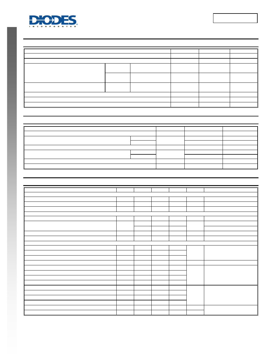
Maximum Ratings
(@T
A
= +25°C, unless otherwise specified.)
Characteristic
Symbol
Value
Unit
Drain-Source Voltage
V
DSS
30 V
Gate-Source Voltage
V
GSS
±20 V
Continuous Drain Current (Note 5) V
GS
= 10V
Steady
State
T
A
= +25°C
T
A
= +70°C
I
D
11
8.5
A
t<10s
T
A
= +25°C
T
A
= +70°C
I
D
14
11
A
Continuous Drain Current (Note 5) V
GS
= 10V
Steady
State
T
C
= +25°C
T
C
= +100°C
I
D
30
20
A
Pulsed Drain Current (10µs pulse, duty cycle = 1%)
I
DM
90 A
Avalanche Current (Notes 6) L = 0.1mH
I
AR
24 A
Repetitive Avalanche Energy (Notes 6) L = 0.1mH
E
AR
29 mJ
Thermal Characteristics
Characteristic Symbol
Value
Units
Total Power Dissipation (Note 4)
P
D
0.9 W
Thermal Resistance, Junction to Ambient (Note 4)
Steady State
R
θJA
140 °C/W
t < 10s
90
°C/W
Total Power Dissipation (Note 5)
P
D
2.4 W
Thermal Resistance, Junction to Ambient (Note 5)
Steady State
R
θJA
52 °C/W
t < 10s
35
°C/W
Thermal Resistance, Junction to Case
R
θJC
4.8 °C/W
Operating and Storage Temperature Range
T
J,
T
STG
-55 to +150
°C
Electrical Characteristics
(@T
A
= +25°C, unless otherwise specified.)
Characteristic
Symbol
Min
Typ
Max
Unit
Test Condition
OFF CHARACTERISTICS (Note 8)
Drain-Source Breakdown Voltage
BV
DSS
30 — — V
V
GS
= 0V, I
D
= 250μA
Zero Gate Voltage Drain Current
I
DSS
—
—
1
μA
V
DS
= 30V, V
GS
= 0V
Gate-Source Leakage
I
GSS
—
—
±100 nA
V
GS
= ±20V, V
DS
= 0V
ON CHARACTERISTICS (Note 8)
Gate Threshold Voltage
V
GS(th)
1.0 — 2.5 V
V
DS
= V
GS
, I
D
= 250μA
Static Drain-Source On-Resistance
R
DS(ON)
—
6.5 8.5
m
Ω
V
GS
= 10V, I
D
= 18A
—
8 10.5
V
GS
= 4.5V, I
D
= 16A
Forward Transfer Admittance
|Y
fs
|
—
20 — S
V
DS
= 5V, I
D
= 18A
Diode Forward Voltage
V
SD
—
0.75 1.0 V
V
GS
= 0V, I
S
= 1A
DYNAMIC CHARACTERISTICS (Note 9)
Input Capacitance
C
iss
—
2075 —
pF
V
DS
= 15V, V
GS
= 0V,
f = 1.0MHz
Output Capacitance
C
oss
—
190
—
Reverse Transfer Capacitance
C
rss
—
138
—
Gate resistance
R
g
—
2.4
—
Ω
V
DS
= 0V, V
GS
= 0V, f = 1.0MHz
Total Gate Charge (V
GS
= 4.5V)
Q
g
—
16.1
—
nC
V
DS
= 15V, I
D
= 18A
Total Gate Charge (V
GS
= 10V)
Q
g
—
37
—
Gate-Source Charge
Q
gs
—
6.1
—
Gate-Drain Charge
Q
gd
—
5.9
—
Turn-On Delay Time
t
D(on)
—
4.5
—
ns
V
DS
= 15V, V
GS
= 10V,
R
L
= 0.83
Ω, R
GEN
= 3
Ω,
Turn-On Rise Time
t
r
—
19.6
—
Turn-Off Delay Time
t
D(off)
—
31
—
Turn-Off Fall Time
t
f
—
10.7
—
Reverse Recovery Time
t
rr
—
13.7
—
ns
I
F
=15A, di/dt=500A/µs
Reverse Recovery Charge
Q
rr
—
18.3 —
nC
Notes:
4. Device mounted on FR-4 PCB with minimum recommended pad layout, single sided.
5. Device mounted on 2” x 2” FR-4 PCB with high coverage 2 oz. Copper, single sided.
6. Repetitive rating, pulse width limited by junction temperature.
7. I
AR
and E
AR
rating are based on low frequency and duty cycles to keep T
J
= +25°C.
8. Short duration pulse test used to minimize self-heating effect.
9. Guaranteed by design. Not subject to production testing.