Maximum ratings, Thermal characteristics, Electrical characteristics – Diodes DMN100 User Manual
Page 2: Dmn100
DMN100
Document number: DS30049 Rev. 9 - 2
2 of 4
March 2012
© Diodes Incorporated
DMN100
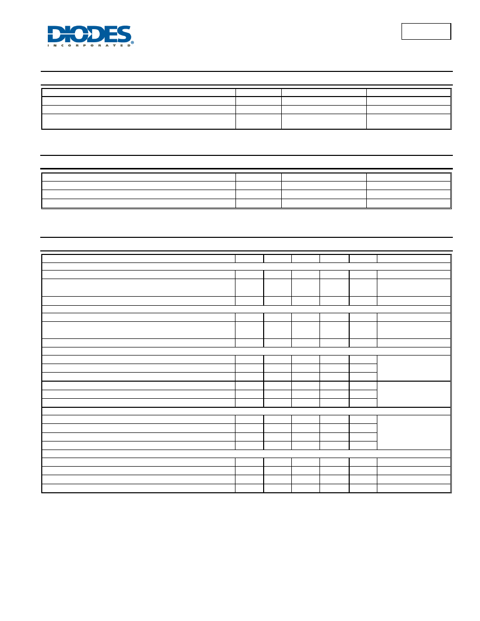
Maximum Ratings
@T
A
= 25°C unless otherwise specified
Characteristic Symbol
Value
Units
Drain-Source Voltage
V
DSS
30 V
Gate-Source Voltage
Continuous
V
GSS
±20
V
Drain Current
Continuous
Pulsed
I
D
1.1
4.0
A
Thermal Characteristics
@T
A
= 25°C unless otherwise specified
Characteristic
Symbol
Value
Units
Total Power Dissipation
P
D
500
mW
Thermal Resistance, Junction to Ambient
R
θJA
250
K/W
Operating and Storage Temperature Range
T
J
, T
STG
-55 to +150
°C
Electrical Characteristics
@T
A
= 25°C unless otherwise specified
Characteristic Symbol
Min
Typ
Max
Unit
Test
Condition
OFF CHARACTERISTICS (Note 4)
Drain-Source Breakdown Voltage
BV
DSS
30 — — V
V
GS
= 0V, I
D
= 250
μA
Zero Gate Voltage Drain Current
@ T
J
= 25°C
@
T
J
= 125°C
I
DSS
—
—
1.0
10
μA
V
DS
= 24V, V
GS
= 0V
Gate-Body Leakage
I
GSS
—
—
± 100
nA
V
GS
=
± 12V, V
DS
= 0V
ON CHARACTERISTICS (Note 4)
Gate Threshold Voltage
V
GS(th)
1.0 — 3.0 V
V
DS
= 10V, I
D
= 1.0mA
Static Drain-Source On-Resistance
R
DS (ON)
— —
0.170
0.150
Ω
V
GS
= 4.5V, I
D
= 0.5A
V
GS
= 10V, I
D
= 1.0A
Forward Transconductance
g
FS
1.3 2.4
⎯
S
V
DS
= 10V, I
D
= 0.5A
DYNAMIC CHARACTERISTICS
Input Capacitance
C
iss
— 150 — pF
V
DS
= 10V, V
GS
= 0V
f = 1.0MHz
Output Capacitance
C
oss
— 90 — pF
Reverse Transfer Capacitance
C
rss
— 30 — pF
Total Gate Charge
Q
g
— 5.5 — nC
V
DS
= 24V, I
D
= 1.0A,
V
GS
= 10V
Gate-to-Source Charge
Q
gs
— 0.8 — nC
Gate-to-Drain Charge
Q
gd
— 1.3 — nC
SWITCHING CHARACTERISTICS
Turn-On Delay Time
t
D(ON)
— 10 — ns
V
DD
= 10V, I
D
= 0.5A,
V
GS
= 5.0V, R
GEN
= 50
Ω
Turn-Off Delay Time
t
D(OFF)
— 25 — ns
Turn-On Rise Time
t
r
— 15 — ns
Turn-Off Fall Time
t
f
— 45 — ns
SOURCE-DRAIN RATINGS (BODY DIODE)
Continuous Source Current
I
S
— — 0.54 A
—
Pulse Source Current
I
SM
— — 4.0 A
—
Forward Voltage
V
SD
— — 1.2 V
I
F
= 1.0A, V
GS
= 0V
Reverse Recovery Time
t
rr
— 35 — ns
I
F
= 1.0A, di/dt = 50A/
μs
Notes:
4. Pulse width
≤ 300μs, duty cycle ≤ 2%.