Diodes DMN2112SN User Manual
Dmn2112sn new prod uc t, Features, Mechanical data
DMN2112SN
Document number: DS30830 Rev. 5 - 2
1 of 4
August 2011
© Diodes Incorporated
DMN2112SN
NEW PROD
UC
T
N-CHANNEL ENHANCEMENT MODE FIELD EFFECT TRANSISTOR
Features
• Low
On-Resistance
•
Ideal for Notebook Computer, Portable Phone, PCMCIA
Cards, and Battery Powered Circuits
•
Lead Free By Design/RoHS Compliant (Note 2)
•
Qualified to AEC-Q101 Standards for High Reliability
•
ESD Protected Gate
•
"Green" Device (Note 3)
Mechanical Data
• Case:
SC59
•
Case Material - Molded Plastic, "Green" Molding Compound.
UL Flammability Classification Rating 94V-0
•
Moisture Sensitivity: Level 1 per J-STD-020C
•
Terminals: Finish Matte Tin annealed over Copper leadframe.
Solderable per MIL-STD-202, Method 208
•
Terminal Connections: See Diagram
•
Marking Information: See Page 3
•
Ordering & Date Code Information: See Page 3
•
Weight: 0.014 grams (approximate)
Maximum Ratings
@T
A
= 25°C unless otherwise specified
Characteristic
Symbol
Value
Units
Drain-Source Voltage
V
DSS
20
V
Gate-Source Voltage
Continuous
V
GSS
± 8
V
Drain
Current
Continuous
Pulsed
I
D
1.2
4.0
A
Thermal Characteristics
@T
A
= 25°C unless otherwise specified
Characteristic
Symbol
Value
Units
Total Power Dissipation
P
d
500
mW
Thermal Resistance, Junction to Ambient
R
θJA
250
°C /W
Operating and Storage Temperature Range
T
j
, T
STG
-55 to +150
°C
Electrical Characteristics
@T
A
= 25°C unless otherwise specified
Characteristic
Symbol
Min
Typ
Max
Unit
Test Condition
OFF CHARACTERISTICS (Note 1)
Drain-Source Breakdown Voltage
BV
DSS
20
⎯
⎯
V
V
GS
= 0V, I
D
= 250µA
Zero Gate Voltage Drain Current
@ T
j
= 25
°C
I
DSS
⎯
⎯
10
µA
V
DS
= 20V, V
GS
= 0V
Gate-Body Leakage
I
GSS
⎯
⎯
± 10
µA
V
GS
=
± 8V, V
DS
= 0V
ON CHARACTERISTICS (Note 1)
Gate Threshold Voltage
V
GS(th)
0.5
⎯
1.2
V
V
DS
= 10V, I
D
= 1.0mA
Static Drain-Source On-Resistance
R
DS (ON)
⎯
⎯
0.10
0.14
0.25
Ω
V
GS
= 4.5V, I
D
= 0.5A
V
GS
= 2.5V, I
D
= 0.5A
V
GS
= 1.5V, I
D
= 0.1A
Forward Transfer Admittance
IY
fs
I
⎯
4.2
⎯
S
V
DS
= 10V, I
D
=0.5A
Diode Forward Voltage
V
SD
⎯
0.8 1.1 V
V
GS
= 0V, I
S
= 1A
DYNAMIC CHARACTERISTICS
Input Capacitance
C
iss
⎯
220
⎯
pF
V
DS
= 10V, V
GS
= 0V
f = 1.0MHz
Output Capacitance
C
oss
⎯
120
⎯
pF
Reverse Transfer Capacitance
C
rss
⎯
45
⎯
pF
SWITCHING CHARACTERISTICS
Turn-On Delay Time
t
D(ON)
⎯
10
⎯
ns
V
DD
= 5V, I
D
= 0.5A,
V
GS
= 10V, R
GEN
= 50
Ω
Turn-Off Delay Time
t
D(OFF)
⎯
75
⎯
ns
Turn-On Rise Time
t
r
⎯
15
⎯
ns
Turn-Off Fall Time
t
f
⎯
65
⎯
ns
Notes:
1. Pulse width
≤ 300μs, duty cycle ≤ 2%.
2. No purposefully added lead.
3. Diodes Inc.'s "Green" Policy can be found on our website at
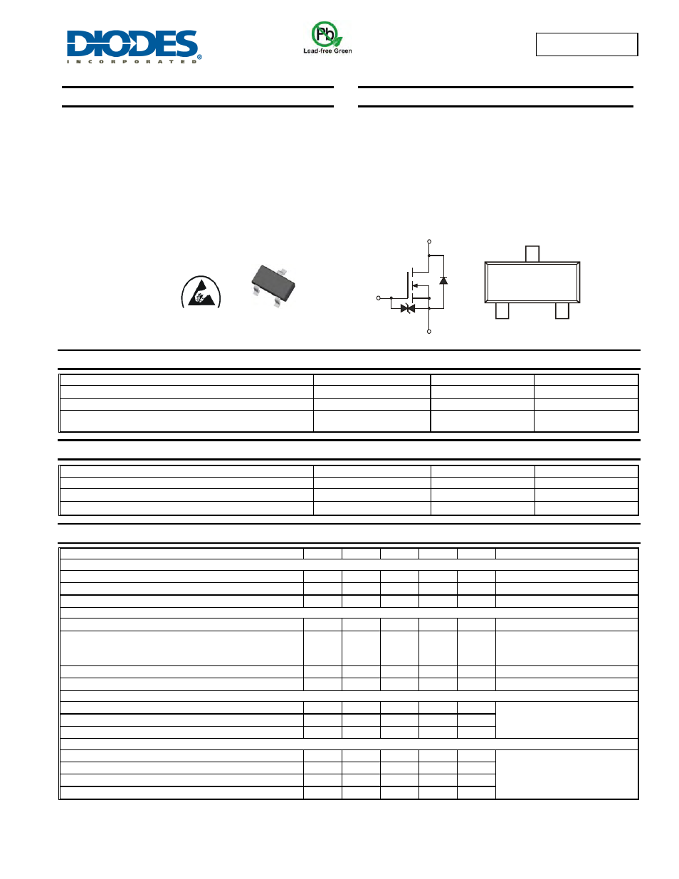
SC59
TOP VIEW
Pin Out Configuration
TOP VIEW
ESD Protected
Source
Gate
Protection
Diode
Gate
Drain
EQUIVALENT CIRCUIT
D
G
S