Maximum ratings, Thermal characteristics, Electrical characteristics – Diodes DMN2005LPK User Manual
Page 2: Dmn2005lpk
DMN2005LPK
Document number: DS30836 Rev. 9 - 2
2 of 6
June 2012
© Diodes Incorporated
DMN2005LPK
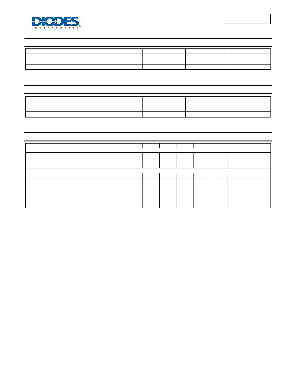
Maximum Ratings
(@T
A
= 25°C unless otherwise specified.)
Characteristic Symbol
Value
Unit
Drain-Source Voltage
V
DSS
20 V
Gate-Source Voltage
V
GSS
±10
V
Drain Current per element (Note 5)
I
D
440 mA
Thermal Characteristics
Characteristic Symbol
Value
Unit
Total Power Dissipation (Note 5)
P
D
450 mW
Thermal Resistance, Junction to Ambient
R
θJA
218
°C/W
Operating and Storage Temperature Range
T
j
, T
STG
-65 to +150
°C
Electrical Characteristics
(@T
A
= 25°C unless otherwise specified.)
Characteristic Symbol
Min
Typ
Max
Unit
Test
Condition
OFF CHARACTERISTICS (Note 6)
Drain-Source Breakdown Voltage
BV
DSS
20
⎯
⎯
V
V
GS
= 0V, I
D
= 100
μA
Zero Gate Voltage Drain Current
I
DSS
⎯
⎯
10 µA
V
DS
= 17V, V
GS
= 0V
Gate-Source Leakage
I
GSS
⎯
⎯
±5
µA
V
GS
=
±8V, V
DS
= 0V
ON CHARACTERISTICS (Note 6)
Gate Threshold Voltage
V
GS(th)
0.53
⎯
1.2 V
V
DS
= V
GS
, I
D
= 100
μA
Static Drain-Source On-Resistance
R
DS (ON)
⎯
⎯
⎯
⎯
⎯
0.35
0.4
0.45
0.55
0.65
1.5
1.7
1.7
3.5
3.5
Ω
V
GS
= 4V, I
D
= 10mA
V
GS
= 2.7V, I
D
= 200mA
V
GS
= 2.5V, I
D
= 10mA
V
GS
= 1.8V, I
D
= 200mA
V
GS
= 1.5V, I
D
= 1mA
Forward Transfer Admittance
|Y
fs
|
40
⎯
⎯
mS
V
DS
= 3V, I
D
= 10mA
Notes:
5. Device mounted on FR-4 PCB.
6. Short duration pulse test used to minimize self-heating effect.