Maximum ratings, Thermal characteristics, Electrical characteristics – Diodes DMN2005DLP4K User Manual
Page 2
DMN2005DLP4K
Document number: DS30801 Rev. 9 - 2
2 of 5
June 2012
© Diodes Incorporated
DMN2005DLP4K
Maximum Ratings
@T
A
= 25°C unless otherwise specified
Characteristic Symbol
Value
Unit
Drain-Source Voltage
V
DSS
20 V
Gate-Source Voltage
V
GSS
±10
V
Drain Current per element (Note 5) Continuous
Pulsed (Note 6)
I
D
300
350
mA
Thermal Characteristics
@T
A
= 25°C unless otherwise specified
Characteristic Symbol
Value
Unit
Total Power Dissipation (Note 5)
P
D
400 mW
Thermal Resistance, Junction to Ambient
R
θJA
231 °C/W
Operating and Storage Temperature Range
T
J
, T
STG
-65 to +150
°C
Electrical Characteristics
@T
A
= 25°C unless otherwise specified
Characteristic Symbol
Min
Typ
Max
Unit
Test
Condition
OFF CHARACTERISTICS (per element) (Note 7)
Drain-Source Breakdown Voltage
BV
DSS
20
⎯
⎯
V
V
GS
= 0V, I
D
= 100
μA
Zero Gate Voltage Drain Current
I
DSS
⎯
⎯
10
μA
V
DS
= 17V, V
GS
= 0V
Gate-Source Leakage
I
GSS
⎯
⎯
±5
μA
V
GS
=
±8V, V
DS
= 0V
ON CHARACTERISTICS (per element) (Note 7)
Gate Threshold Voltage
V
GS(th)
0.53
⎯
0.9 V
V
DS
= V
GS
, I
D
= 100
μA
Static Drain-Source On-Resistance
R
DS (ON)
⎯
⎯
⎯
⎯
⎯
0.35
0.4
0.45
0.55
0.65
1.5
1.7
1.7
3.5
3.5
Ω
V
GS
= 4V, I
D
= 10mA
V
GS
= 2.7V, I
D
= 200mA
V
GS
= 2.5V, I
D
= 10mA
V
GS
= 1.8V, I
D
= 200mA
V
GS
= 1.5V, I
D
= 1mA
Forward Transfer Admittance
⏐Y
fs
⏐
40
⎯
⎯
mS
V
DS
= 3V, I
D
= 10mA
Notes:
5. Device mounted on FR-4 PCB.
6. Pulse width
≤10μS, Duty Cycle ≤1%.
7. Short duration pulse test used to minimize self-heating effect.
0
0.5
1.0
1.5
2.0
0
1
2
3
4
5
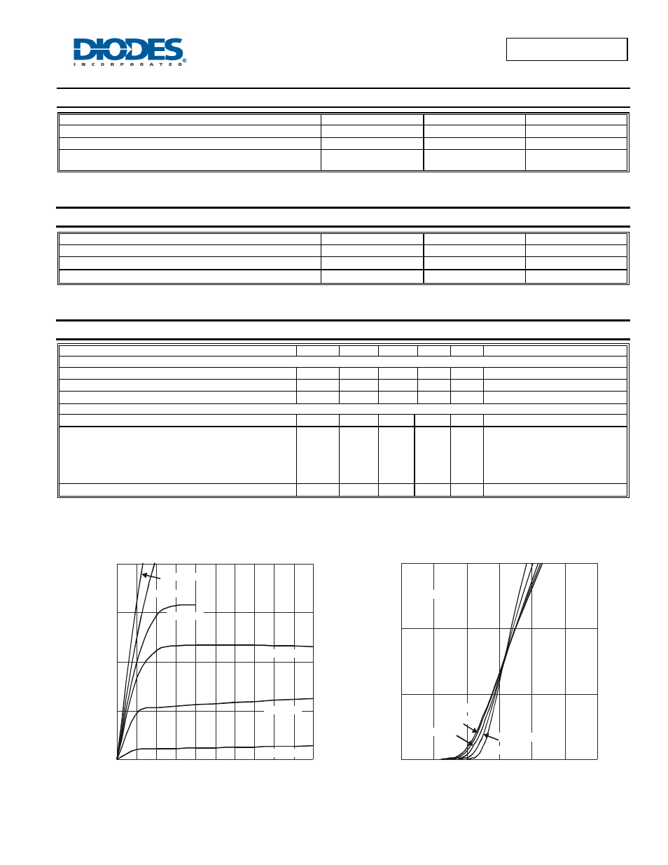
Figure 1 Typical Output Characteristics
V
, DRAIN-SOURCE VOLTAGE (V)
DS
I,
D
R
AI
N
C
U
R
R
E
N
T
(A
)
D
V
= 1.5V
GS
V
= 2.0V
GS
V
= 2.5V
GS
V
= 4.5V
GS
V
= 1.2V
GS
V
= 1.8V
GS
0
0.5
1.0
1.5
0
0.5
1
1.5
2
2.5
3
I,
D
R
AI
N
C
U
R
R
EN
T
(A
)
D
Figure 2 Typical Transfer Characteristics
V
, GATE SOURCE VOLTAGE (V)
GS
V
= 5V
DS
T = -55°C
A
T = 25°C
A
T = 125°C
A
T = 150°C
A
T = 85°C
A