Electrical characteristics, Dmmt3904w – Diodes DMMT3904W User Manual
Page 3
DMMT3904W
Document number: DS30311 Rev. 12 - 2
3 of 6
May 2014
© Diodes Incorporated
DMMT3904W
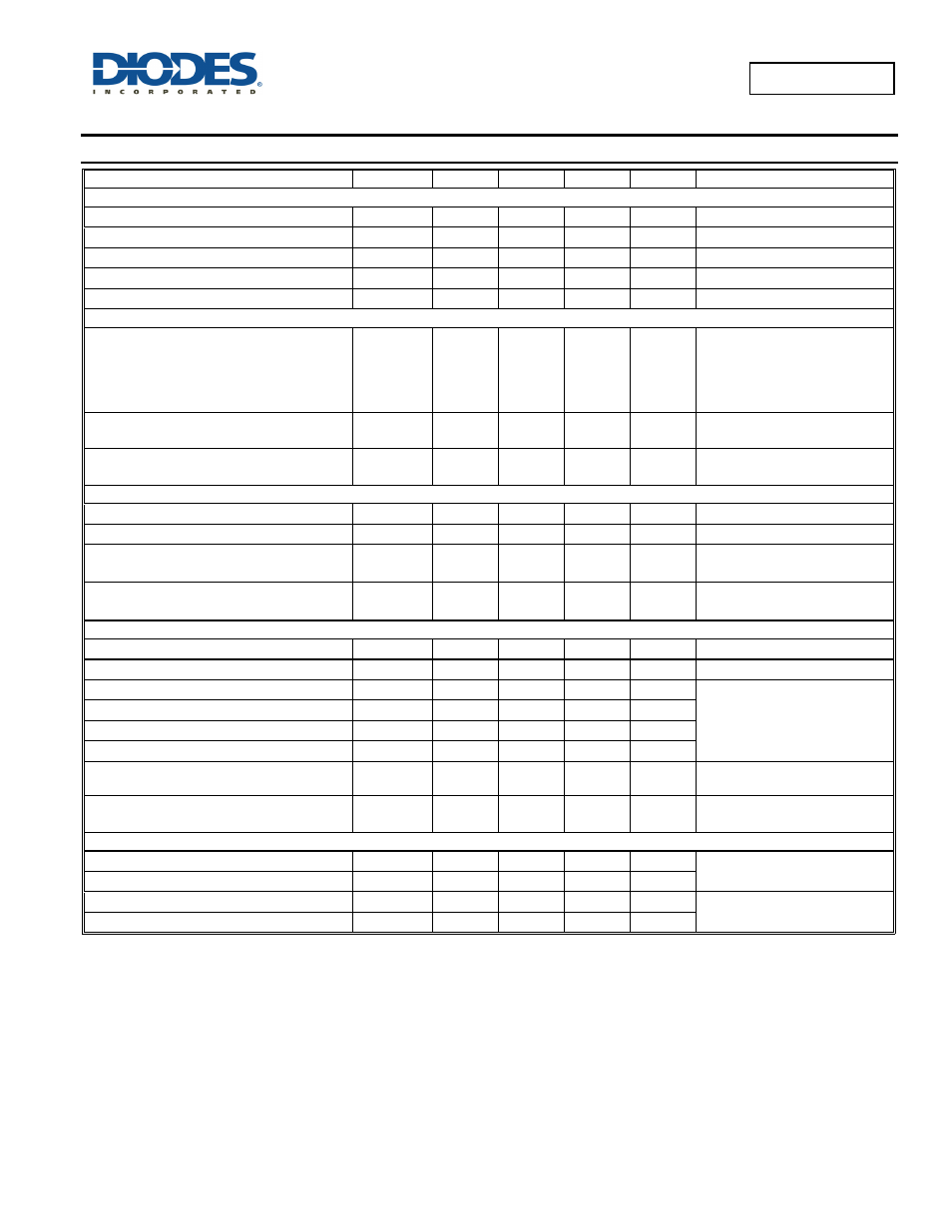
Electrical Characteristics
(@T
A
= +25°C unless otherwise specified.)
Characteristic
Symbol
Min
Typ
Max
Unit
Test Condition
OFF CHARACTERISTICS
Collector-Base Breakdown Voltage
BV
CBO
60
⎯
⎯
V
I
C
= 100
μA, I
E
= 0
Collector-Emitter Breakdown Voltage(Note 9)
BV
CEO
40
⎯
⎯
V
I
C
= 1.0mA, I
B
= 0
Emitter-Base Breakdown Voltage
BV
EBO
6.0
⎯
⎯
V
I
E
= 100µA, I
C
= 0
Collector Cutoff Current
I
CEX
⎯
⎯
50
nA
V
CE
= 30V, V
EB(OFF)
= 3.0V
Base Cutoff Current
I
BL
⎯
⎯
50
nA
V
CE
= 30V, V
EB(OFF)
= 3.0V
ON CHARACTERISTICS (Note 9)
DC Current Gain
h
FE
40
70
100
60
30
⎯
⎯
⎯
300
⎯
⎯
⎯
I
C
= 100µA, V
CE
= 1.0V
I
C
= 1.0mA, V
CE
= 1.0V
I
C
= 10mA, V
CE
= 1.0V
I
C
= 50mA, V
CE
= 1.0V
I
C
= 100mA, V
CE
= 1.0V
Collector-Emitter Saturation Voltage
V
CE(SAT)
⎯
⎯
200
300
mV
I
C
= 10mA, I
B
= 1.0mA
I
C
= 50mA, I
B
= 5.0mA
Base-Emitter Saturation Voltage
V
BE(SAT)
0.65
⎯
⎯
850
950
mV
I
C
= 10mA, I
B
= 1.0mA
I
C
= 50mA, I
B
= 5.0mA
MATCHING CHARACTERISTICS
DC Current Gain Matching (Note 10
)
h
FE1
/
h
FE2
⎯
1
2
%
I
C
= 2mA, V
CE
= 5V
Base-Emitter Voltage Matching (Note 11
)
V
BE1
-
V
BE2
⎯
1 2 mV
I
C
= 2mA, V
CE
= 5V
Collector-Emitter Saturation Voltage (Note 10)
V
CE(SAT)1
/
V
CE(SAT)2
⎯
1 2 %
I
C
= 10mA, I
B
= 1.0mA
Base-Emitter Saturation Voltage (Note 10)
V
BE(SAT)1
/
V
BE(SAT)2
⎯
1 2 %
I
C
= 10mA, I
B
= 1.0mA
SMALL SIGNAL CHARACTERISTICS
Output Capacitance
C
obo
⎯
⎯
4.0
pF
V
CB
= 5.0V, f = 1.0MHz, I
E
= 0
Input Capacitance
C
ibo
⎯
⎯
8.0
pF
V
EB
= 0.5V, f = 1.0MHz, I
C
= 0
Input Impedance
h
ie
1.0
⎯
10
k
Ω
V
CE
= 10V, I
C
= 1.0mA,
f = 1.0kHz
Voltage Feedback Ratio
h
re
0.5
⎯
8
x 10
-4
Small Signal Current Gain
h
fe
100
⎯
400
⎯
Output Admittance
h
oe
1.0
⎯
40
μS
Current Gain-Bandwidth Product
f
T
300
⎯
⎯
MHz
V
CE
= 20V, I
C
= 10mA,
f = 100MHz
Noise Figure
NF
⎯
⎯
5.0
dB
V
CE
= 5.0V, I
C
= 100
μA,
R
S
= 1.0k
Ω,
f = 1.0kHz
SWITCHING CHARACTERISTICS
Delay Time
t
d
⎯
⎯
35
ns
V
CC
= 3.0V, I
C
= 10mA,
V
BE(off)
= -0.5V, I
B1
= 1.0mA
Rise Time
t
r
⎯
⎯
35
ns
Storage Time
t
s
⎯
⎯
200
ns
V
CC
= 3.0V, I
C
= 10mA,
I
B1
= I
B2
= 1.0mA
Fall Time
t
f
⎯
⎯
50
ns
Note:
9. Measured under pulsed conditions. Pulse width ≤ 300µs. Duty cycle ≤ 2%.
10. Is the ratio of one transistor compared to the other transistor.
11. V
BE1
-
V
BE2
is the absolute difference of one transistor compared to the other transistor.