Fcx605 – Diodes FCX605 User Manual
Page 5
ISSUE 2 - SEPTEMBER 2005
FCX605
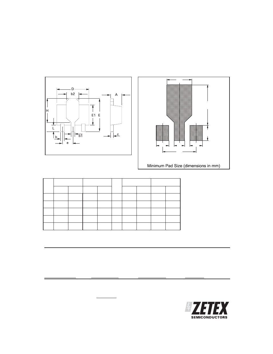
PACKAGE DIMENSIONS
PAD LAYOUT DETAILS
5
1.2
1.0
1.2
3.2
1.5
4.0
2.4
SOT89 pattern.
Europe
Zetex GmbH
Streitfeldstraße 19
D-81673 München
Germany
Telefon: (49) 89 45 49 49 0
Fax: (49) 89 45 49 49 49
Americas
Zetex Inc
700 Veterans Memorial Hwy
Hauppauge, NY 11788
USA
Telephone: (1) 631 360 2222
Fax: (1) 631 360 8222
Asia Pacific
Zetex (Asia) Ltd
3701-04 Metroplaza Tower 1
Hing Fong Road, Kwai Fong
Hong Kong
Telephone: (852) 26100 611
Fax: (852) 24250 494
Corporate Headquarters
Zetex Semiconductors plc
Zetex Technology Park
Chadderton, Oldham, OL9 9LL
United Kingdom
Telephone (44) 161 622 4444
Fax: (44) 161 622 4446
These offices are supported by agents and distributors in major countries world-wide.
This publication is issued to provide outline information only which (unless agreed by the Company in writing) may not be used, applied or reproduced for
any purpose or form part of any order or contract or be regarded as a representation relating to the products or services concerned. The Company reserves
the right to alter without notice the specification, design, price or conditions of supply of any product or service.
For the latest product information, log on to
www.zetex.com
© Zetex Semiconductors plc 2005
DIM
Millimeters
Inches
DIM
Millimeters
Inches
Min
Max
Min
Max
Min
Max
Min
Max
A
1.40
1.60
0.550
0.630
e
1.40
1.50
0.055
0.059
b
0.38
0.48
0.015
0.019
E
3.75
4.25
0.150
0.167
b1
-
0.53
-
0.021
E1
-
2.60
-
0.102
b2
1.50
1.80
0.060
0.071
G
2.90
3.00
0.114
0.118
c
0.28
0.44
0.011
0.017
H
2.60
2.85
0.102
0.112
PACKAGE DIMENSIONS