Diodes DDTCxxxxLP (R1≠R2 Series) User Manual
Features, Mechanical data, Maximum ratings
DDTCxxxxLP (R1
≠R2 Series)
Document number: DS30755 Rev. 7 - 2
1 of 7
March 2009
© Diodes Incorporated
DDTCxxxxLP (R1
≠R2 Series)
PRE-BIASED SMALL SIGNAL SURFACE MOUNT 100mA NPN TRANSISTOR
Features
•
Epitaxial Planar Die Construction
•
Ultra-Small Leadless Surface Mount Package
•
Ideally Suited for Automated Assembly Processes
•
Lead Free By Design/RoHS Compliant (Note 1)
•
"Green" Device (Note 2)
•
Qualified to AEC-Q101 Standards for High Reliability
Part Number
R1 (NOM)
R2 (NOM)
DDTC123JLP 2.2K
47K
DDTC143ZLP 4.7K
47K
DDTC114YLP 10K
47K
Mechanical Data
• Case:
DFN1006-3
•
Case Material: Molded Plastic, "Green" Molding Compound.
UL Flammability Classification Rating 94V-0
•
Moisture Sensitivity: Level 1 per J-STD-020D
•
Terminal Connections: Collector Dot (See Diagram and
Marking Information)
• Terminals:
Finish
⎯ NiPdAu over Copper leadframe.
Solderable per MIL-STD-202, Method 208
•
Marking Information: See Page 6
•
Ordering Information: See Page 6
•
Weight: 0.0009 grams (approximate)
Maximum Ratings
@T
A
= 25°C unless otherwise specified
Characteristic
P/N
Symbol
Value
Unit
Supply Voltage
V
CC
50
V
Input Voltage
DDTC123JLP
V
IN
-5 to +12
V
DDTC143ZLP
-5 to +30
DDTC114YLP
-5 to +40
Output Voltage
DDTC123JLP
I
O
100
mA
DDTC143ZLP
100
DDTC114YLP
70
Maximum Collector Current
I
C(MAX)
100
mA
Thermal Characteristics
Characteristic
Symbol
Value
Unit
Power Dissipation (Note 3)
P
D
250
mW
Power Deration above 25
°C
P
der
2
mW/
°C
Thermal Resistance, Junction to Ambient Air (Note 3)
(Equivalent to one heated junction of NPN)
R
θJA
500
°C/W
Operating and Storage Temperature Range
T
J
, T
STG
-55 to +150
°C
Notes:
1. No purposefully added lead.
2. Diodes Inc.'s "Green" policy can be found on our website at
3. Device mounted on FR-4 PCB, 1 inch x 0.85 inch x 0.062 inch; pad layout as shown on Diodes Inc. suggested pad layout document AP02001, which
can be found on page 6 or our website at
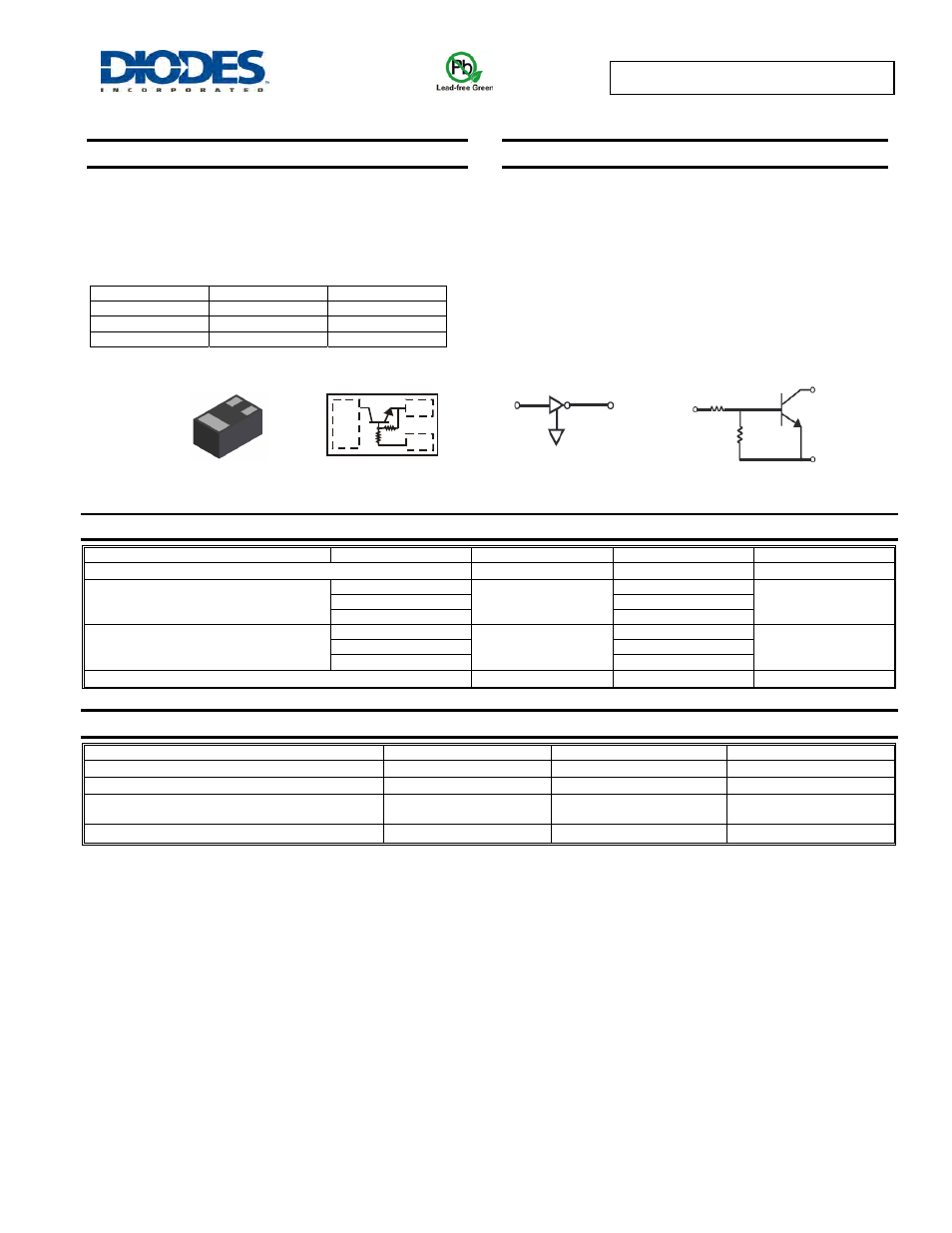
Bottom View
Device Schematics
Package Pin Out
Configuration
1
B
C
E
2
3
IN
R
1
R
2
OUT
GND
IN
B
1
2
3
C
E
GND
OUT
C
1
2
3
R
1
R
2
E
B