Diodes DDTC (R1≠R2 SERIES) E User Manual
Ddtc (r1 r2 series) e, Features, Mechanical data
DDTC (R1 R2 SERIES) E
≠
NPN PRE-BIASED SMALL SIGNAL SURFACE MOUNT TRANSISTOR
Features
DS30314 Rev. 9 - 2
1 of 4
www.diodes.com
DDTC (R1
≠R2 SERIES) E
© Diodes Incorporated
•
Epitaxial Planar Die Construction
•
Complementary PNP Types Available (DDTA)
•
Built-In Biasing Resistors, R1
≠R2
•
Lead Free/RoHS Compliant (Note 2)
•
"Green" Device (Note 3 and 4)
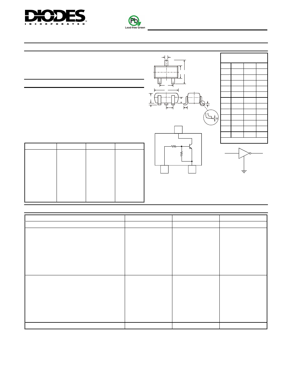
Mechanical Data
•
Case: SOT-523
•
Case Material: Molded Plastic. UL Flammability Classification
Rating 94V-0
•
Moisture Sensitivity: Level 1 per J-STD-020C
•
Terminals: Solderable per MIL-STD-202, Method 208
•
Lead Free Plating (Matte Tin Finish annealed over Alloy 42
leadframe)
•
Terminal Connections: See Diagram
•
Marking & Date Code Information: See Table Below & Page 4
•
Ordering Information: See Page 4
•
Weight: 0.002 grams (approximate)
P/N
R1 (NOM)
R2 (NOM)
Marking
DDTC113ZE
DDTC123YE
DDTC123JE
DDTC143XE
DDTC143FE
DDTC143ZE
DDTC114YE
DDTC114WE
DDTC124XE
DDTC144VE
DDTC144WE
1K
Ω
2.2K
Ω
2.2K
Ω
4.7K
Ω
4.7K
Ω
4.7K
Ω
10K
Ω
10K
Ω
22K
Ω
47K
Ω
47K
Ω
10K
Ω
10K
Ω
47K
Ω
10K
Ω
22K
Ω
47K
Ω
47K
Ω|
4.7K
Ω
47K
Ω
10K
Ω
22K
Ω
N02
N05
N06
N09
N10
N11
N14
N15
N18
N21
N22
SOT-523
A
M
J
L
D
Dim
Min
Max Typ
A
0.15
0.30 0.22
B
0.75
0.85 0.80
C
1.45
1.75 1.60
D — — 0.50
G 0.90 1.10 1.00
H
1.50
1.70 1.60
J
0.00
0.10 0.05
K
0.60
0.80 0.75
L
0.10
0.30 0.22
M 0.10 0.20 0.12
N 0.45 0.65 0.50
α
0
°
8
°
—
All Dimensions in mm
C
B
Maximum Ratings
@T
A
= 25°C unless otherwise specified
Characteristic
Symbol
Value
Unit
Supply Voltage (3) to (2)
V
CC
50
V
Input Voltage, (1) to (2)
DDTC113ZE
DDTC123YE
DDTC123JE
DDTC143XE
DDTC143FE
DDTC143ZE
DDTC114YE
DDTC114WE
DDTC124XE
DDTC144VE
DDTC144WE
V
IN
-5 to +10
-5 to +12
-5 to +12
-7 to +20
-6 to +30
-5 to +30
-6 to +40
-10 to +30
-10 to +40
-15 to +40
-10 to +40
V
Output Current
DDTC113ZE
DDTC123YE
DDTC123JE
DDTC143XE
DDTC143FE
DDTC143ZE
DDTC114YE
DDTC114WE
DDTC124XE
DDTC144VE
DDTC144WE
I
O
100
100
100
100
100
100
70
100
50
30
30
mA
Output Current All
I
C
(Max)
100
mA
Notes:
1. Mounted on FR4 PC Board with recommended pad layout at http://www.diodes.com/datasheets/ap02001.pdf.
2. No purposefully added lead.
3. Diodes Inc.'s "Green" policy can be found on our website at http://www.diodes.com/products/lead_free/index.php.
4. Product manufactured with Date Code UO (week 40, 2007) and newer are built with Green Molding Compound. Product manufactured prior to Date
Code UO are built with Non-Green Molding Compound and may contain Halogens or Sb2O3 Fire Retardants.
Schematic and Pin Configuration
Equivalent Inverter Circuit
1
3
2
GND (0)
C
B
IN
OUT
E
H
K
G
TOP VIEW
N
R1
OUT
B
C
E
R2
3
2
1
IN
GND(0)