Diodes DDTA (R1≠R2 SERIES) User Manual
Ddta (r1 ≠ r2 series), Features, Mechanical data
DDTA (R1
≠R2 SERIES) E
Document number: DS30318 Rev. 8 - 2
1 of 6
November 2011
© Diodes Incorporated
DDTA (R1
≠R2 SERIES)
PNP PRE-BIASED SMALL SIGNAL SURFACE MOUNT TRANSISTOR
Features
•
Epitaxial Planar Die Construction
•
Complementary NPN Types Available (DDTC)
•
Built-In Biasing Resistors, R1
≠R2
•
“Lead Free”, RoHS Compliant (Note 1)
•
Halogen and Antimony Free "Green" Device (Note 2)
•
Qualified to AEC-Q101 Standards for High Reliability
Part Number
R1 (NOM)
R2 (NOM)
Marking
DDTA113ZE
1K
Ω 10KΩ
P02
DDTA123YE
2.2K
Ω 10KΩ
P05
DDTA123JE
2.2K
Ω 47KΩ
P06
DDTA143XE
4.7K
Ω 10KΩ
P09
DDTA143FE
4.7K
Ω 22KΩ
P10
DDTA143ZE
4.7K
Ω 47KΩ
P11
DDTA114YE
10K
Ω 47KΩ
P14
DDTA114WE
10K
Ω 4.7KΩ
P15
DDTA124XE
22K
Ω 47KΩ
P18
DDTA144VE
47K
Ω 10KΩ
P21
DDTA144WE
47K
Ω 22KΩ
P22
Mechanical Data
• Case:
SOT523
•
Case Material: Molded Plastic, “Green” Molding Compound,
Note 3. UL Flammability Classification Rating 94V-0
•
Moisture Sensitivity: Level 1 per J-STD-020
•
Terminals: Matte Tin Finish annealed over Alloy 42 leadframe
(Lead Free Plating) Solderable per MIL-STD-202, Method 208
•
Weight: 0.002 grams (approximate)
Ordering Information
(Note 3)
Part Number
Case
Packaging
DDTA113ZE-7-F
SOT523
3000/Tape & Reel
DDTA123YE-7-F
SOT523
3000/Tape & Reel
DDTA123JE-7-F
SOT523
3000/Tape & Reel
DDTA143XE-7-F
SOT523
3000/Tape & Reel
DDTA143FE-7-F
SOT523
3000/Tape & Reel
DDTA143ZE-7-F
SOT523
3000/Tape & Reel
DDTA114YE-7-F
SOT523
3000/Tape & Reel
DDTA114WE-7-F
SOT523
3000/Tape & Reel
DDTA124XE-7-F
SOT523
3000/Tape & Reel
DDTA144VE-7-F
SOT523
3000/Tape & Reel
DDTA144WE-7-F
SOT523
3000/Tape & Reel
Notes:
1. No purposefully added lead.
2. Diodes Inc.'s "Green" policy can be found on our w3. For packaging details, go to our website at
Marking Information
Date Code Key
Year
2005
2006
2007
2008
2009
2010
2011
2012
2013
2014
2015
Code
S T U V W X Y Z A B C
Month
Jan
Feb
Mar
Apr
May
Jun
Jul
Aug
Sep
Oct
Nov
Dec
Code
1 2 3 4 5 6 7 8 9 O N D
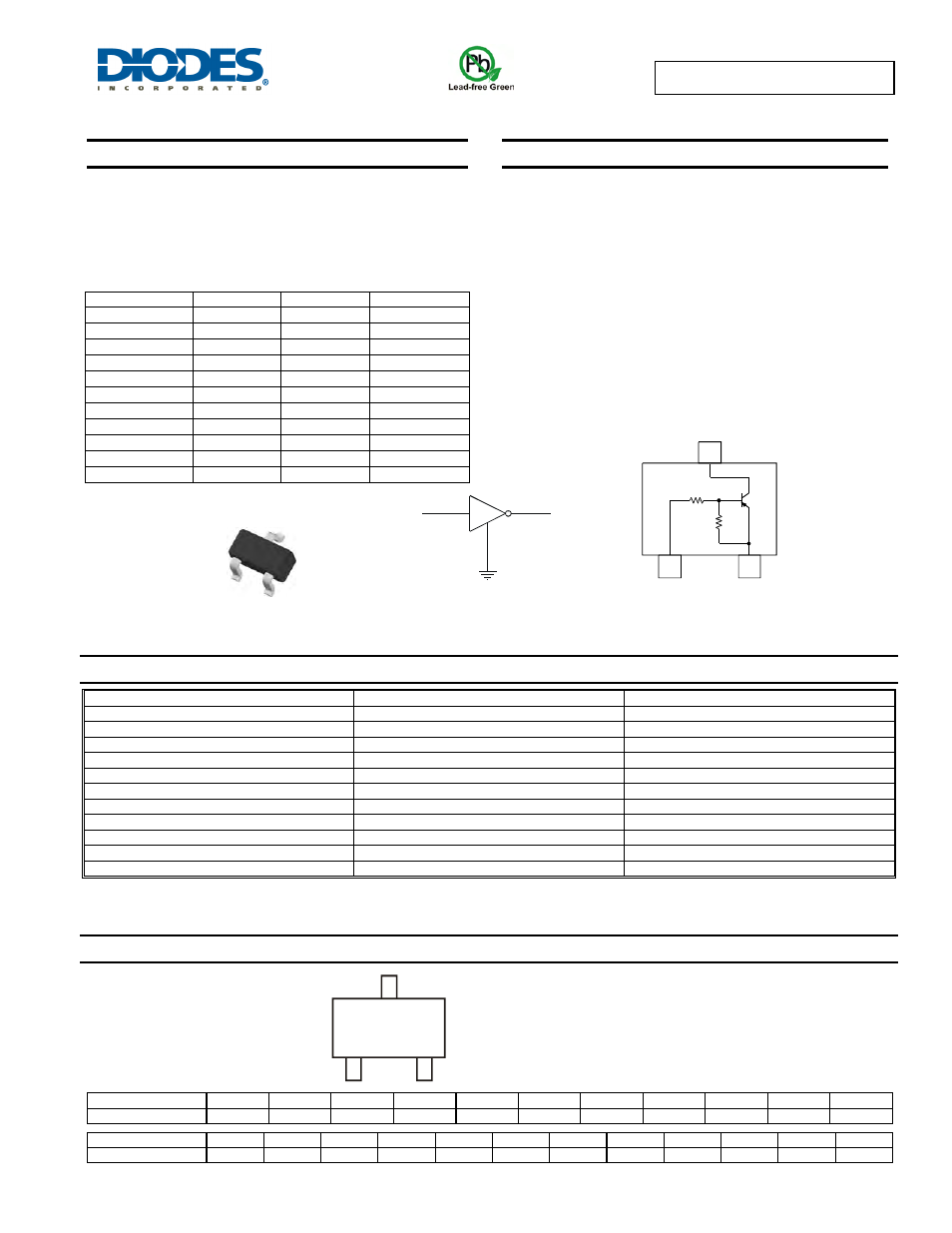
Top View
Device Schematic
Package Pin Out
Configuration
1
3
2
GND (+)
C
B
IN
OUT
E
R1
OUT
B
C
E
R2
3
2
1
IN
GND(+)
Pxx = Product Type Marking Code (See Features Table)
YM = Date Code Marking
Y = Year (ex: T = 2006)
M = Month (ex: 9 = September)
Pxx
YM
SOT523