Diodes FMMT451 User Manual
Fmmt451, Typical characteristics, Absolute maximum ratings
SOT23 NPN SILICON PLANAR
HIGH PERFROMANCE TRANSISTOR
ISSUE 3 - OCTOBER 1995
✪
FEATURES
* Low equivalent on-resistance; R
CE(sat)
400m
Ω
at 1A
* 1 Amp continuous current
* P
tot
= 500 mW
COMPLEMENTARY TYPE FMMT551
PARTMARKING DETAIL
451
ABSOLUTE MAXIMUM RATINGS.
PARAMETER
SYMBOL
VALUE
UNIT
Collector-Base Voltage
V
CBO
80
V
Collector-Emitter Voltage
V
CEO
60
V
Emitter-Base Voltage
V
EBO
5
V
Peak Pulse Current
I
CM
2
A
Continuous Collector Current
I
C
1
A
Base Current
I
B
200
mA
Power Dissipation at T
amb
=25°C
P
tot
500
mW
Operating and Storage Temperature Range
T
j
:T
stg
-55 to +150
°C
ELECTRICAL CHARACTERISTICS (at T
amb
= 25°C).
PARAMETER
SYMBOL
MIN. MAX.
UNIT
CONDITIONS.
Collector-Base
Breakdown Voltage
V
(BR)CBO
80
V
I
C
=100
µ
A
Collector-Emitter
Sustaining Voltage
V
CEO(sus)
60
V
I
C
=10mA*
Emitter-Base Breakdown
Voltage
V
(BR)EBO
5
V
I
E
=100
µ
A
Collector Cut-Off Current I
CBO
0.1
µ
A
V
CB
=60V
Emitter Cut-Off Current
I
EBO
0.1
µ
A
V
EB
=4V
Collector-Emitter
Saturation Voltage
V
CE(sat)
0.35
V
I
C
=150mA, I
B
=15mA*
Base-Emitter
Saturation Voltage
V
BE(sat)
1.1
V
I
C
=150mA, I
B
=15mA*
Static Forward Current
Transfer Ratio
h
FE
50
10
150
I
C
=150mA, V
CE
=10V*
I
C
=1A, V
CE
=10V*
Transition
Frequency
f
T
150
MHz
I
C
=50mA, V
CE
=10V
f=100MHz
Output Capacitance
C
obo
15
pF
V
CB
=10V, f=1MHz
*Measured under pulsed conditions. Pulse width=300
µ
s. Duty cycle
≤
2%
FMMT451
C
B
E
3 - 109
3 - 108
FMMT451
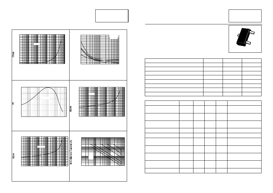
TYPICAL CHARACTERISTICS
V
CE(sat)
v I
C
I
C
-
Collector Current (Amps)
V
- (
Vol
ts
)
I
C
-
Collector Current (Amps)
I
C
-
Collector Current (Amps)
h
FE
v I
C
V
BE(sat)
v I
C
I
C
-
Collector Current (Amps)
V
BE(on)
v I
C
h
V
- (
Vol
ts
)
V
- (V
ol
ts
)
40
80
120
160
200
0
10
0.2
0.4
0.6
0.8
Switching Speeds
I
C
-
Collector Current (Amps)
S
w
itch
in
g t
im
e
0.001
0.01
0.1
1
I
C
/I
B
=10
0.1
1
I
B1
=I
B2
=I
C
/10
0.01
ts
tf
td
tr
ts
ns
tf,tr,td
ns
100
50
150
0
V
CE
=2V
0
I
C
/I
B
=10
0.2
0.4
0.8
1.0
1.2
1.4
1.6
1.8
0.6
V
CE
=2V
ts
tf
td
tr
800
400
200
600
0
0.001
1
0.01
0.1
10
0.2
0.4
0.8
1.0
1.2
1.4
1.6
1.8
0.6
0.001
1
0.01
0.1
10
0.001
1
0.01
0.1
10
V
CE
=10V
100
Single Pulse Test at Tamb=25°C
10
1
Safe Operating Area
V
CE
- Collector Emitter Voltage (V)
1
10
0.1
0.1
0.01
1s
DC
100ms
10ms
100
µ
s
1ms