Maximum ratings, Thermal characteristics – Diodes DXT2012P5 User Manual
Page 2
DXT2012P5
Document number: DS32070 Rev. 2 - 2
2 of 7
March 2010
© Diodes Incorporated
DXT2012P5
PowerDI is a registered trademark of Diodes
ADVAN
CE I
N
F
O
RM
ATI
O
N
A Product Line of
Diodes Incorporated
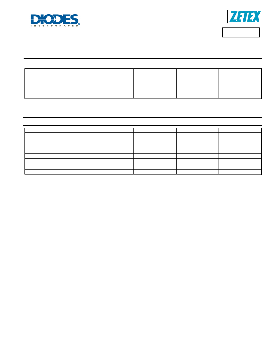
Maximum Ratings
@T
A
= 25°C unless otherwise specified
Characteristic Symbol
Value
Unit
Collector-Base Voltage
V
CBO
-100 V
Collector-Emitter Voltage
V
CEO
-60 V
Emitter-Base Voltage
V
EBO
-7 V
Continuous Collector Current
I
C
-5.5 A
Peak Pulse Current
I
CM
-15 A
Thermal Characteristics
Characteristic Symbol
Value
Unit
Power Dissipation @ T
A
= 25°C (Note 4)
P
D
3.2 W
Thermal Resistance, Junction to Ambient Air (Note 4) @T
A
= 25°C
R
θJA
39 °C/W
Power Dissipation @ T
A
= 25°C (Note 5)
P
D
1.7 W
Thermal Resistance, Junction to Ambient Air (Note 5) @T
A
= 25°C
R
θJA
75 °C/W
Power Dissipation @ T
A
= 25°C (Note 6)
P
D
0.74 W
Thermal Resistance, Junction to Ambient Air (Note 6) @T
A
= 25°C
R
θJA
169 °C/W
Thermal Resistance, Junction to Collector Terminal
R
θJT
5.6 °C/W
Operating and Storage Temperature Range
T
J
, T
STG
-55 to +150
°C
Notes:
4. Device mounted on FR-4 PCB, single sided 2 oz. copper, collector pad dimensions 50mm x 50mm.
5. Device mounted on FR-4 PCB, single sided 1 oz. copper, collector pad dimensions 25mm x 25mm.
6. Device mounted on FR-4 PCB, 2 single sided 1oz. copper, minimum recommended pad layout.