Maximum ratings, Thermal characteristics, Electrical characteristics – Diodes DPBT8105 User Manual
Page 2: Dpbt8105
DPBT8105
Document number: DS30514 Rev. 9 - 2
2 of 5
June 2011
© Diodes Incorporated
DPBT8105
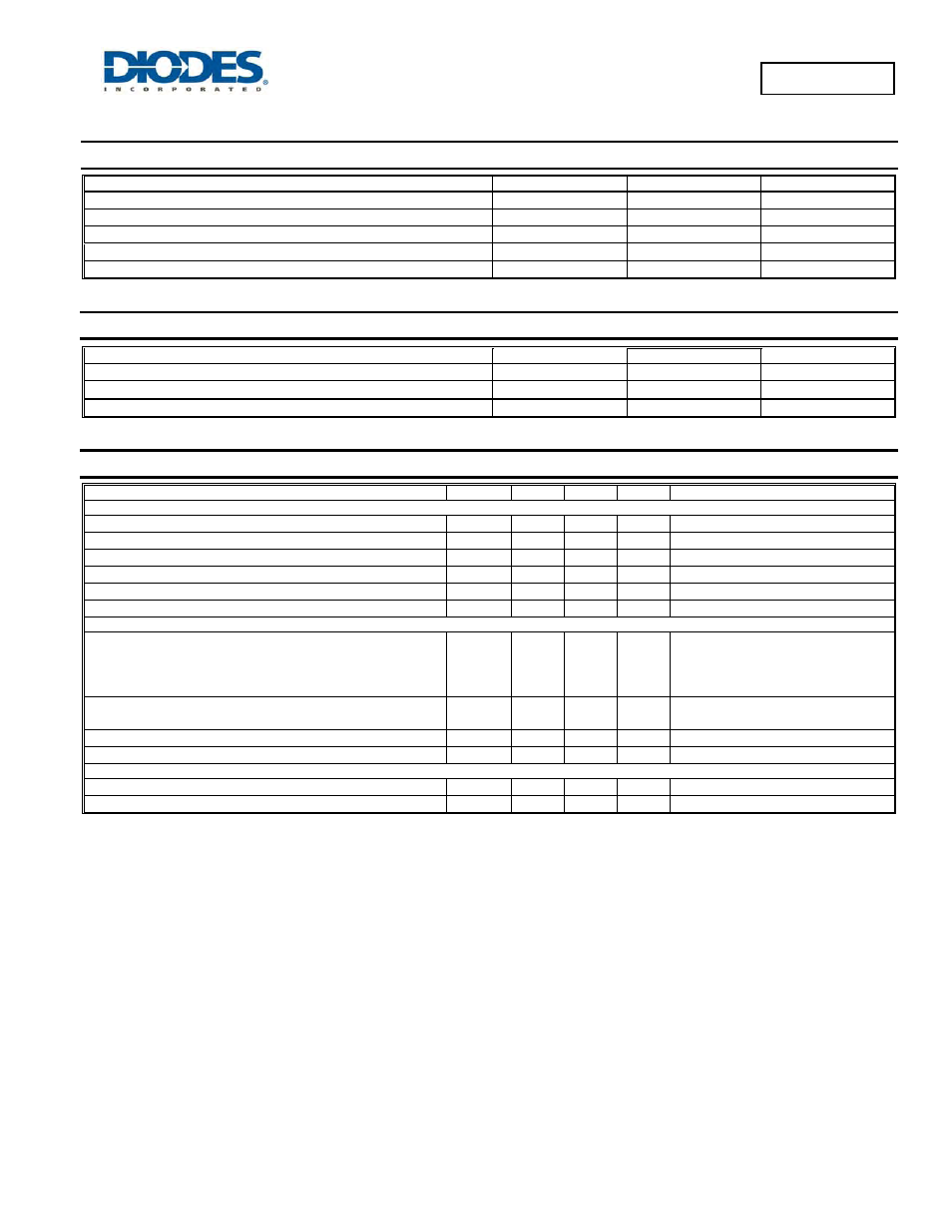
Maximum Ratings
@T
A
= 25°C unless otherwise specified
Characteristic
Symbol
Value
Unit
Collector-Base Voltage
V
CBO
-80
V
Collector-Emitter Voltage
V
CEO
-60
V
Emitter-Base Voltage
V
EBO
-5
V
Collector Current - Continuous
I
C
-1
A
Peak Pulse Collector Current
I
CM
-2 A
Thermal Characteristics
Characteristic
Symbol Value Unit
Power Dissipation (Note 4) @ T
A
= 25
°C
P
D
600
mW
Thermal Resistance, Junction to Ambient (Note 4) @ T
A
= 25
°C
R
θJA
209
°C/W
Operating and Storage Temperature Range
T
J
, T
STG
-55 to +150
°C
Electrical Characteristics
@T
A
= 25°C unless otherwise specified
Characteristic
Symbol
Min
Max
Unit
Test Condition
OFF CHARACTERISTICS (Note 5)
Collector-Base Breakdown Voltage
V
(BR)CBO
-80
⎯
V
I
C
= -100
μA, I
E
= 0
Collector-Emitter Breakdown Voltage
V
(BR)CEO
-60
⎯
V
I
C
= -10mA, I
B
= 0
Emitter-Base Breakdown Voltage
V
(BR)EBO
-5
⎯
V
I
E
= -100
μA, I
C
= 0
Collector Cutoff Current
I
CBO
⎯
-100
nA
V
CB
= -60V, I
E
= 0
Collector Cutoff Current
I
CES
⎯
-100 nA
V
CE
= -60V
Emitter Cutoff Current
I
EBO
⎯
-100
nA
V
EB
= -4V, I
C
= 0
ON CHARACTERISTICS (Note 5)
DC Current Gain
h
FE
100
100
80
30
⎯
300
⎯
⎯
⎯
I
C
= -1mA, V
CE
= -5V
I
C
= -500mA, V
CE
= -5V
I
C
= -1A, V
CE
= -5V
I
C
= -2A, V
CE
= -5V
Collector-Emitter Saturation Voltage
V
CE(SAT)
⎯
⎯
-0.3
-0.6
V
I
C
= -500mA, I
B
= -50mA
I
C
= -1A, I
B
= -100mA
Base-Emitter Saturation Voltage
V
BE(SAT)
⎯
-1.2 V
I
C
= -1A, I
B
= -100mA
Base-Emitter Turn On Voltage
V
BE(ON)
⎯
-1.0 V
I
C
= -1A, V
CE
= -5V
SMALL SIGNAL CHARACTERISTICS
Output Capacitance
C
obo
⎯
12
pF
V
CB
= -10V, f = 1.0MHz
Current Gain-Bandwidth Product
f
T
150
⎯
MHz
V
CE
= 10V, I
C
= 50mA, f = 100MHz
Notes:
4. Device mounted on FR-4 PCB, 1 inch x 0.85 inch x 0.062 inch; pad layout as shown on Diodes Inc. suggested pad layout document AP02001, which
can be found on our website5. Short duration pulse test used to minimize self-heating effect.