Diodes IMT17 User Manual
Imt17, Features, Mechanical data
IMT17
Document number: DS31202 Rev. 4 - 2
1 of 4
March 2009
© Diodes Incorporated
IMT17
DUAL PNP SMALL SIGNAL SURFACE MOUNT TRANSISTOR
Features
•
Epitaxial Planar Die Construction
•
Small Surface Mount Package
•
Lead Free By Design/RoHS Compliant (Note 1)
•
"Green" Device (Note 2)
Mechanical Data
• Case:
SOT-26
•
Case Material: Molded Plastic, “Green” Molding Compound.
UL Flammability Classification Rating 94V-0
•
Moisture Sensitivity: Level 1 per J-STD-020D
•
Terminal Connections: See Diagram
•
Terminals: Finish – Matte Tin Annealed Over Copper Leadframe.
Solderable per MIL-STD-202, Method 208
•
Marking Information: See Page 3
•
Ordering Information: See Page 3
•
Weight: 0.016 grams (approximate)
Maximum Ratings
@T
A
= 25°C unless otherwise specified
Characteristic Symbol
Value
Unit
Collector-Base Voltage
V
CBO
-60 V
Collector-Emitter Voltage
V
CEO
-50 V
Emitter-Base Voltage
V
EBO
-5.0 V
Continuous Collector Current
I
C
-500 mA
Thermal Characteristics
Characteristic Symbol
Value
Unit
Power Dissipation (Note 3) @T
A
= 25°C
P
D
300 mW
Thermal Resistance, Junction to Ambient Air (Note 3) @T
A
= 25°C
R
θJA
417
°C /W
Operating and Storage Temperature Range
T
J
, T
STG
-55 to +150
°C
Electrical Characteristics
@T
A
= 25°C unless otherwise specified
Characteristic Symbol
Min
Typ
Max
Unit
Test
Condition
OFF CHARACTERISTICS (Note 4)
Collector-Base Breakdown Voltage
V
(BR)CBO
-60 — —
V I
C
= -100
μA
Collector-Emitter Breakdown Voltage
V
(BR)CEO
-50 — —
V I
C
= -1.0mA
Emitter-Base Breakdown Voltage
V
(BR)EBO
-5.0 — —
V I
E
= -100
μA
Collector Cutoff Current
I
CBO
— — -0.1
μA
V
CB
= -30V
Emitter Cutoff Current
I
EBO
— — -0.1
μA
V
EB
= -4.0V
ON CHARACTERISTICS (Note 4)
DC Current Gain
h
FE
120 — 390
— V
CE
= -3.0V, I
C
= -100mA
Collector-Emitter Saturation Voltage (Note 3)
V
CE(SAT)
— — -0.6
V I
C
= -500mA, I
B
= -50mA
SMALL SIGNAL CHARACTERISTICS
Gain Bandwidth Product
f
T
— 200 —
MHz
V
CE
= -5V, I
E
= 20mA,
f = 100MHz
Output Capacitance
C
ob
— 7 — pF
V
CB
= -10V, I
E
= 0, f = 1MHz
Notes:
1. No purposefully added lead.
2. Diodes Inc.'s "Green" policy can be found on our websit
3. Device mounted on FR-4 PCB; pad layout as shown on Diodes Inc. suggested pad layout document AP02001, which can be found on page 4 or on our
website4. Short duration pulse test used to minimize self-heating effect.
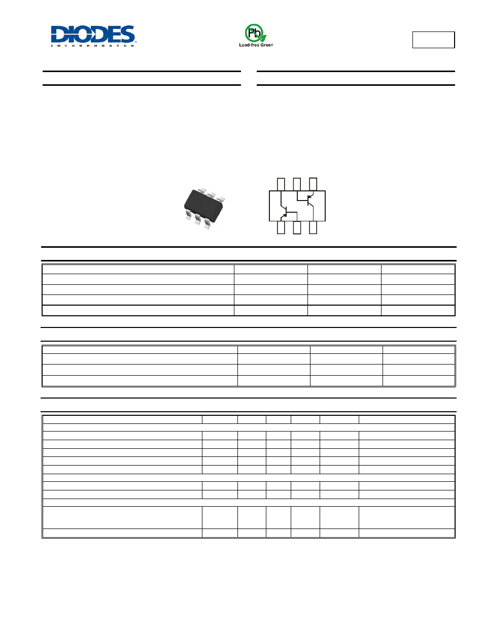
Top View
Device Schematic
E2
C2
C1
E1
B2
B1