Maximum ratings, Thermal characteristics, Dss5540x – Diodes DSS5540X User Manual
Page 2
DSS5540X
Document number: DS31653 Rev. 2 - 2
2 of 5
October 2010
© Diodes Incorporated
DSS5540X
Maximum Ratings
@T
A
= 25°C unless otherwise specified
Characteristic Symbol
Value
Unit
Collector-Base Voltage
V
CBO
-40 V
Collector-Emitter Voltage
V
CEO
-40 V
Emitter-Base Voltage
V
EBO
-6 V
Peak Pulse Collector Current
I
CM
-10 A
Repetitive Peak Pulse Collector Current (Note 4)
I
CRP
-5 A
Continuous Collector Current
I
C
-4 A
Peak Pulse Base Current
I
BM
-2 A
Continuous Base Current
I
B
-1 A
Thermal Characteristics
Characteristic Symbol
Value
Unit
Power Dissipation (Note 5) @ T
A
= 25°C
P
D
0.9 W
Thermal Resistance, Junction to Ambient Air (Note 5) @ T
A
= 25°C
R
θJA
139 °C/W
Power Dissipation (Note 6) @ T
A
= 25°C
P
D
2 W
Thermal Resistance, Junction to Ambient Air (Note 6) @ T
A
= 25°C
R
θJA
62.5 °C/W
Operating and Storage Temperature Range
T
J
, T
STG
-55 to +150
°C
Notes:
4. Pulse width
≤ 10ms; Duty cycle ≤ 0.2
5. Device mounted on FR-4 PCB with minimum recommended pad layout.
6. Device mounted on FR-4 PCB with 1inch
2
copper pad layout.
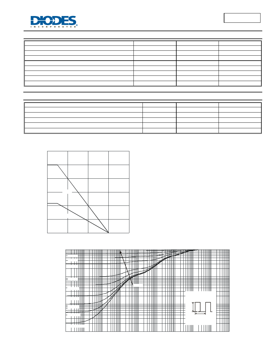
0
0.4
0.8
1.2
2.4
0
50
100
150
200
T , AMBIENT TEMPERATURE ( C)
A
°
Fig. 1 Power Dissipation vs. Ambient Temperature
P
,
P
O
WE
R
DI
S
S
IP
A
T
IO
N (
W
)
D
Note 6
Note 5
1.6
2.0
0.00001 0.0001
0.001
0.01
0.1
1
10
100
1,000
10,000
Fig. 2 Transient Thermal Response
t , PULSE DURATION TIME (s)
1
0.001
0.01
0.1
1
r(t
),
T
R
ANS
IEN
T
T
H
E
R
MA
L
R
ES
IS
T
AN
C
E
T - T = P * R
(t)
Duty Cycle, D = t /t
J
A
JA
1 2
θ
R
(t) = r(t) *
θJA
R
R
= 135°C/W
θ
θ
JA
JA
P(pk)
t
1
t
2
D = 0.7
D = 0.5
D = 0.3
D = 0.05
D = 0.02
D = 0.01
D = 0.005
D = Single Pulse
D = 0.9
D = 0.1