Dss4540x new prod uc t, Electrical characteristics, Dss4540x – Diodes DSS4540X User Manual
Page 2
DSS4540X
Document number: DS31592 Rev. 2 - 2
2 of 4
December 2008
© Diodes Incorporated
DSS4540X
NEW PROD
UC
T
Electrical Characteristics
@T
A
= 25°C unless otherwise specified
Characteristic Symbol
Min
Typ
Max
Unit
Test
Conditions
OFF CHARACTERISTICS
Collector-Base Breakdown Voltage
V
(BR)CBO
40
⎯
⎯
V
I
C
= 100
μA
Collector-Emitter Breakdown Voltage (Note 6)
V
(BR)CEO
40
⎯
⎯
V
I
C
= 10mA
Emitter-Base Breakdown Voltage
V
(BR)EBO
6
⎯
⎯
V
I
E
= 100
μA
Collector-Base Cutoff Current
I
CBO
⎯
⎯
100 nA
V
CB
= 30V, I
E
= 0
⎯
⎯
50
μA
V
CB
= 30V, I
E
= 0, T
A
= 150°C
Collector-Emitter Cut-Off Current
I
CES
⎯
⎯
100 nA
V
CE
= 30V, V
BE
= 0V
Emitter-Base Cutoff Current
I
EBO
⎯
⎯
100 nA
V
EB
= 5V, I
C
= 0
ON CHARACTERISTICS (Note 6)
DC Current Gain
h
FE
300
⎯
⎯
⎯
V
CE
= 2V, I
C
= 0.5A
300
⎯
⎯
V
CE
= 2V, I
C
= 1A
250
⎯
⎯
V
CE
= 2V, I
C
= 2A
100
⎯
⎯
V
CE
= 2V, I
C
= 5A
Collector-Emitter Saturation Voltage
V
CE(SAT)
⎯
⎯
90
mV
I
C
= 0.5A, I
B
= 5mA
⎯
⎯
120
I
C
= 1A, I
B
= 10mA
⎯
80 150
I
C
= 2A, I
B
= 200mA
⎯
160 290
I
C
= 4A, I
B
= 200mA
⎯
185 355
I
C
= 5A, I
B
= 500mA
Equivalent On-Resistance
R
CE(SAT)
⎯
37 71
m
Ω I
C
= 5A, I
B
= 500mA
Base-Emitter Saturation Voltage
V
BE(SAT)
⎯
⎯
1.1
V
I
C
= 4A, I
B
= 200mA
⎯
⎯
1.2
I
C
= 5A, I
B
= 500mA
Base-Emitter Turn-on Voltage
V
BE(ON)
⎯
⎯
1.1 V
V
CE
= 2V, I
C
= 2A
SMALL SIGNAL CHARACTERISTICS
Transition Frequency
f
T
70
⎯
⎯
MHz
V
CE
= 10V, I
C
= 0.1A,
f = 100MHz
Collector Capacitance
C
c
⎯
⎯
75 pF
V
CB
= 10V, I
E
= 0A,
f = 1MHz
SWITCHING CHARACTERISTICS
Turn-On Time
t
on
⎯
135
⎯
ns
V
CC
= 10V, I
C
= 2A,
I
B1
=
40mA
Delay Time
t
d
⎯
60
⎯
ns
Rise Time
t
r
⎯
75
⎯
ns
Turn-Off Time
t
off
⎯
670
⎯
ns
V
CC
= 10V, I
C
= 2A,
I
B1
= I
B2
= 40mA
Storage Time
t
s
⎯
570
⎯
ns
Fall Time
t
f
⎯
100
⎯
ns
Notes:
6. Measured under pulsed conditions. Pulse width = 300
μs. Duty cycle ≤2%.
0
0
P
,
PO
W
E
R D
IS
S
IP
A
T
IO
N (
W
)
D
T , AMBIENT TEMPERATURE ( C)
A
°
Note 4
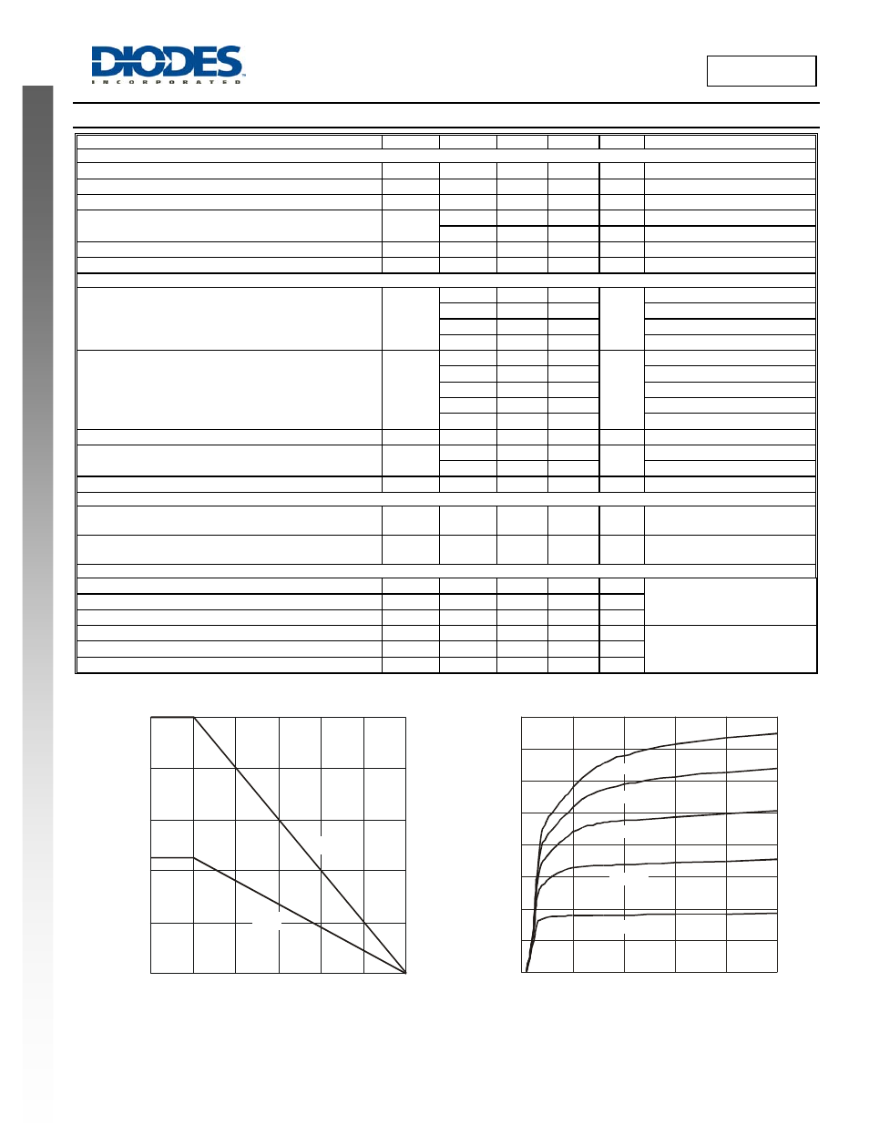
Fig. 1 Power Dissipation vs. Ambient Temperature
0.4
0.8
1.2
1.6
2.0
25
50
75
100
125
150
Note 5
0
0.5
1.0
1.5
2.0
2.5
3.0
3.5
4.0
0
1
2
3
4
5
V
, COLLECTOR-EMITTER VOLTAGE (V)
CE
Fig. 2 Typical Collector Current
vs. Collector-Emitter Voltage
I,
C
O
LL
E
C
T
O
R
C
U
R
R
E
N
T
(A
)
C
I = 2mA
B
I = 4mA
B
I = 6mA
B
I = 8mA
B
I = 10mA
B