Dss4240t new prod uc t, Maximum ratings, Thermal characteristics – Diodes DSS4240T User Manual
Page 2: Electrical characteristics
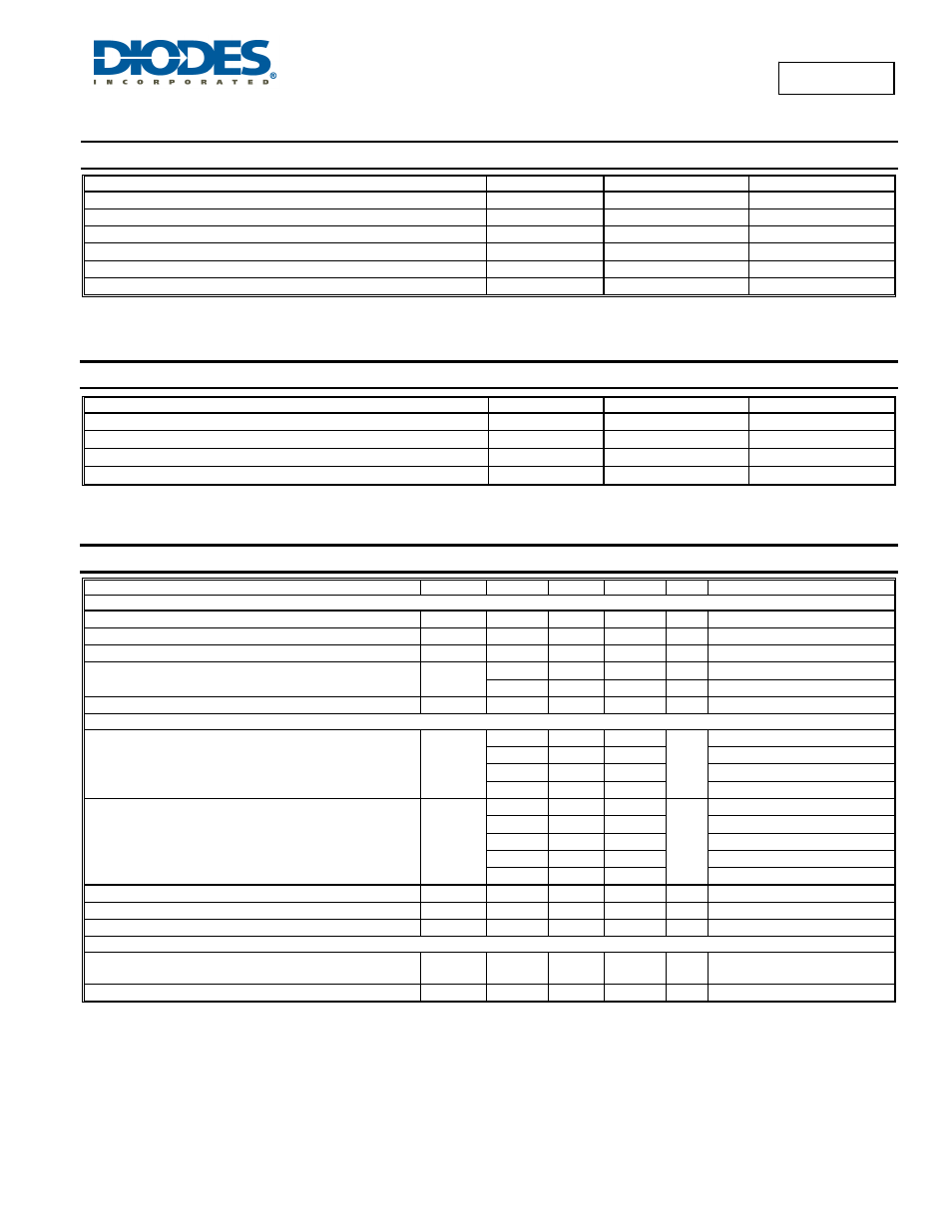
DSS4240T
Document number: DS31623 Rev. 4 - 2
2 of 5
November 2011
© Diodes Incorporated
DSS4240T
NEW PROD
UC
T
Maximum Ratings
@T
A
= 25°C unless otherwise specified
Characteristic Symbol
Value
Unit
Collector-Base Voltage
V
CBO
40 V
Collector-Emitter Voltage
V
CEO
40 V
Emitter-Base Voltage
V
EBO
5 V
Peak Pulse Collector Current
I
CM
3 A
Continuous Collector Current
I
C
2 A
Peak Base Current
I
BM
0.3 A
Thermal Characteristics
@T
A
= 25°C unless otherwise specified
Characteristic Symbol
Value
Unit
Power Dissipation (Note 4)
P
D
600 mW
Thermal Resistance, Junction to Ambient Air (Note 4)
R
θJA
209 °C/W
Thermal Resistance, Junction to Lead (Note 5)
R
θJC
74.95 °C/W
Operating and Storage Temperature Range
T
J
, T
STG
-55 to +150
°C
Electrical Characteristics
@T
A
= 25°C unless otherwise specified
Characteristic Symbol
Min
Typ
Max
Unit
Test
Conditions
OFF CHARACTERISTICS
Collector-Base Breakdown Voltage
BV
CBO
40
⎯
⎯
V
I
C
= 100
μA
Collector-Emitter Breakdown Voltage (Note 6)
BV
CEO
40
⎯
⎯
V
I
C
= 10mA
Emitter-Base Breakdown Voltage
BV
EBO
5
⎯
⎯
V
I
E
= 100
μA
Collector-Base Cutoff Current
I
CBO
⎯
⎯
100
nA
V
CB
= 30V, I
E
= 0
⎯
⎯
50
μA V
CB
= 30V, I
E
= 0, T
A
= 150°C
Emitter-Base Cutoff Current
I
EBO
⎯
⎯
100 nA
V
EB
= 4V, I
C
= 0
ON CHARACTERISTICS (Note 6)
DC Current Gain
h
FE
350
⎯
⎯
⎯
V
CE
= 2V, I
C
= 0.1A
300
⎯
⎯
V
CE
= 2V, I
C
= 0.5A
300
⎯
⎯
V
CE
= 2V, I
C
= 1A
150
⎯
⎯
V
CE
= 2V, I
C
= 2A
Collector-Emitter Saturation Voltage
V
CE(sat)
⎯
⎯
70
mV
I
C
= 100mA, I
B
= 1mA
⎯
30 100
I
C
= 500mA, I
B
= 50mA
⎯
⎯
180
I
C
= 750mA, I
B
= 15mA
⎯
⎯
180
I
C
= 1A, I
B
= 50mA
⎯
⎯
320
I
C
= 2A, I
B
= 200mA
Equivalent On-Resistance
R
CE(sat)
⎯
60 200
m
Ω I
C
= 500mA, I
B
= 50mA
Base-Emitter Saturation Voltage
V
BE(sat)
⎯
⎯
1.1 V
I
C
= 2A, I
B
= 200mA
Base-Emitter Turn-on Voltage
V
BE(on)
⎯
⎯
0.75 V
V
CE
= 2V, I
C
= 100mA
SMALL SIGNAL CHARACTERISTICS
Transition Frequency
f
T
100
⎯
⎯
MHz
V
CE
= 10V, I
C
= 100mA,
f = 100MHz
Output Capacitance
C
ob
⎯
⎯
20 pF
V
CB
= 10V, f = 1MHz
Notes:
4. Device mounted on FR-4 PCB with minimum recommended pad layout.
5. Thermal resistance from junction to solder-point (at the end of the collector lead).
6. Measured under pulsed conditions. Pulse width = 300
μs. Duty cycle ≤ 2%.