Diodes DP0150BDJ User Manual
Features, Mechanical data, Maximum ratings
DP0150ADJ / DP0150BDJ
Document number: DS31485 Rev. 3 - 2
1 of 4
April 2009
© Diodes Incorporated
DP0150ADJ / DP0150BDJ
NEW PROD
UC
T
DUAL PNP SURFACE MOUNT TRANSISTOR
Features
•
Epitaxial Planar Die Construction
•
Ideally Suited for Automated Assembly Processes
•
Lead Free By Design/RoHS Compliant (Note 1)
•
"Green" Device (Note 2)
•
Ultra Small Package
Mechanical Data
• Case:
SOT-963
•
Case Material: Molded Plastic, “Green” Molding Compound. UL
Flammability Classification Rating 94V-0
•
Moisture Sensitivity: Level 1 per J-STD-020D
• Terminals:
Finish
⎯ Matte Tin annealed over Copper leadframe.
Solderable per MIL-STD-202, Method 208
•
Marking Information: See Page 3
•
Ordering Information: See Page 3
•
Weight: 0.0027 grams (approximate)
Maximum Ratings
@T
A
= 25°C unless otherwise specified
Characteristic Symbol
Value
Unit
Collector-Base Voltage
V
CBO
-50 V
Collector-Emitter Voltage
V
CEO
-50 V
Emitter-Base Voltage
V
EBO
-5 V
Collector Current - Continuous
I
C
-100 mA
Base Current
I
B
-30 mA
Thermal Characteristics
Characteristic Symbol
Value
Unit
Power Dissipation (Note 3)
P
D
300 mW
Thermal Resistance, Junction to Ambient (Note 3)
R
θJA
417 °C/W
Operating and Storage Temperature Range
T
J
, T
STG
-55 to +150
°C
Electrical Characteristics
@T
A
= 25°C unless otherwise specified
Characteristic
Symbol
Min
Typ
Max
Unit
Test Condition
OFF CHARACTERISTICS (Note 4)
Collector-Base Breakdown Voltage
V(
BR)CBO
-50 — — V
I
C
= -10
μA, I
E
= 0
Collector-Emitter Breakdown Voltage
V(
BR)CEO
-50 — — V
I
C
= -1mA, I
B
= 0
Emitter-Base Breakdown Voltage
V(
BR)EBO
-5 — — V
I
E
= -10
μA, I
C
= 0
Collector Cut-Off Current
I
CBO
— — -0.1
μA
V
CB
= -50V, I
E
= 0
Emitter Cut-Off Current
I
EBO
— — -0.1
μA
V
EB
= -5V, I
C
= 0
ON CHARACTERISTICS (Note 4)
Collector-Emitter Saturation Voltage
V
CE(SAT)
— -0.15 -0.3 V
I
C
= -100mA, I
B
= -10mA
DC Current Gain DP0150ADJ
DP0150BDJ
h
FE
120 — 240
—
V
CE
= -6V, I
C
= -2mA
200 — 400
SMALL SIGNAL CHARACTERISTICS
Transition Frequency
f
T
80 — —
MHz
V
CE
= -10V, I
E
= 1mA
f = 30MHz
Output Capactiance
C
ob
— 1.6 — pF
V
CB
= -10V, I
E
= 0,
f = 1MHz
Notes:
1. No purposefully added lead.
2. Diodes Inc.'s "Green" policy can be found on our websit3. Device mounted on FR-4 PCB with minimum recommended pad layout.
4. Measured under pulsed conditions. Pulse width = 300µs. Duty cycle
≤2%
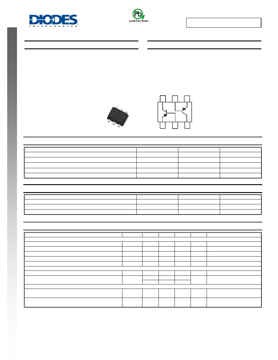
Device Schematic
Top View
SOT-963
6
Q1
Q2
5
4
3
1
2