Fzt789a, Maximum ratings, Thermal characteristics – Diodes FZT789A User Manual
Page 2: Esd ratings
FZT789A
Document Number DS33168 Rev. 5 - 2
2 of 7
January 2013
© Diodes Incorporated
FZT789A
A Product Line of
Diodes Incorporated
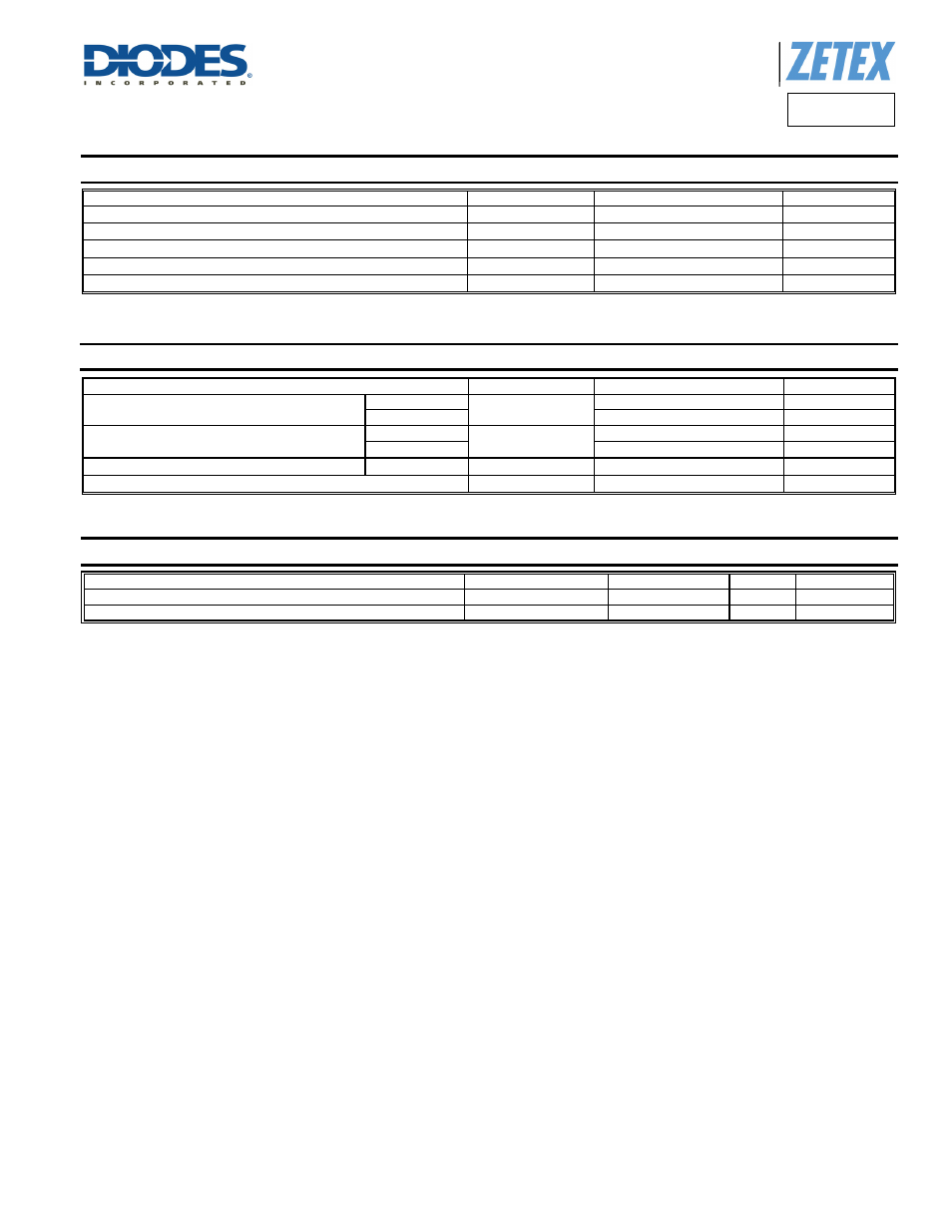
Maximum Ratings
(@T
A
= +25°C, unless otherwise specified.)
Characteristic Symbol
Value
Unit
Collector-Base Voltage
V
CBO
-30 V
Collector-Emitter Voltage
V
CEO
-25 V
Emitter-Base Voltage
V
EBO
-7 V
Continuous Collector Current
I
C
-3 A
Peak Pulse Current
I
CM
-6 A
Thermal Characteristics
(@T
A
= +25°C, unless otherwise specified.)
Characteristic Symbol
Value
Unit
Power Dissipation
(Note 6)
P
D
2 W
(Note 7)
3
W
Thermal Resistance, Junction to Ambient
(Note 6)
R
θJA
62.5
°C/W
(Note 7)
41.7
°C/W
Thermal Resistance, Junction to Leads
(Note 8)
R
θJL
12.93
°C/W
Operating and Storage Temperature Range
T
J,
T
STG
-55 to +150
°C
ESD Ratings
(Note 9)
Characteristic Symbol
Value
Unit
JEDEC
Class
Electrostatic Discharge - Human Body Model
ESD HBM
4,000
V
3A
Electrostatic Discharge - Machine Model
ESD MM
≥ 400
V
C
Notes:
6. For a device surface mounted on 25mm X 25mm FR4 PCB with high coverage of single sided 1 oz copper, in still air conditions; device measured when
operating in steady state condition.
7. Same as note (6), except the device is mounted on 50mm X 50mm single sided 2oz weight copper.
8. Thermal resistance from junction to solder-point (at the end of the collector lead).
9. Refer to JEDEC specification JESD22-A114 and JESD22-A115.