Diodes DLPA004 User Manual
Dlpa004 new prod uc t, Features, Data line transient protection
DLPA004
Document number: DS31593 Rev. 4 - 2
1 of 4
www.diodes.com
March 2009
© Diodes Incorporated
DLPA004
NEW PROD
UC
T
DATA BUS TRANSIENT SUPPRESSOR
Features
•
Fast Switching Speed
•
Ultra-Small Surface Mount Package
•
Lead Free By Design/RoHS Compliant (Note 3)
•
"Green" Device (Note 4)
•
Qualified to AEC-Q101 Standards for High Reliability
Data Line Transient Protection
In accordance with (Note 1):
•
IEC 61000-4-2 Contact Method: ±15kV
•
IEC 61000-4-2 Air Discharge Method: ±25kV
Mechanical Data
• Case:
SOT-363
•
Case Material: Molded Plastic, "Green" Molding Compound.
UL Flammability Classification Rating 94V-0 (Note 3)
•
Moisture Sensitivity: Level 1 per J-STD-020D
• Terminals:
Finish
⎯ Matte Tin annealed over Alloy 42
Leadframe. Solderable per MIL-STD-202, Method 208
•
Ordering Information: See Page 3
•
Marking Information: See Page 3
•
Weight: 0.006 grams (approximate)
Maximum Ratings
@T
A
= 25°C unless otherwise specified
Characteristic Symbol
Value
Unit
Peak Repetitive Reverse Voltage
Working Peak Reverse Voltage
DC Blocking Voltage
V
RRM
V
RWM
V
R
85 V
RMS Reverse Voltage
V
R(RMS)
60 V
Forward Current (Single Diode)
I
FM
200 mA
Peak Forward Surge Current
8.3ms Single half Sine-Wave Superimposed on Rated Load
I
FM(surge)
3.5 A
Average Rectified Forward Current (Note 1)
I
F(AV)
1 A
Repetitive Peak Forward Current
I
FRM
450 mA
Non-Repetitive Peak Forward Surge Current
@ t = 1.0
μs
@ t = 1.0ms
@ t = 1.0s
I
FSM
4.0
1.0
0.5
A
Thermal Characteristics
Characteristic Symbol
Value
Unit
Power Dissipation (Note 2)
P
D
200 mW
Thermal Resistance Junction to Ambient Air (Note 2)
R
θJA
625
°C/W
Operating and Storage Temperature Range
T
J
, T
STG
-65 to +150
°C
Notes:
1. Tested with V
CC
pins connected to GND pin.
2. Device mounted on FR-4 PCB, 1 inch x 0.85 inch x 0.062 inch; pad layout as shown on Diodes Inc. suggested pad layout document AP02001, which
can be found on our website3. No purposefully added lead.
4. Diodes Inc.'s "Green" policy can be found on our websit
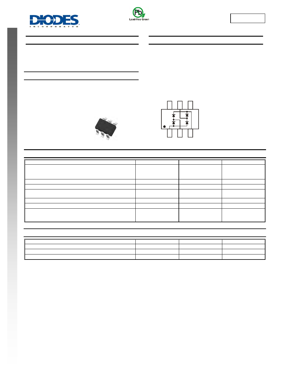
TOP VIEW
SOT-363
Device Schematic
5
4
6
2
3
1
I/O
N/C
N/C
V
N
V
P
I/O