Es3a/ab - es3d/db, Maximum ratings, Thermal characteristics – Diodes ES3A/AB - ES3D/DB User Manual
Page 2: Electrical characteristics
ES3A/AB - ES3D/DB
Document number: DS14003 Rev. 15 - 2
2 of 4
November 2010
© Diodes Incorporated
ES3A/AB - ES3D/DB
Maximum Ratings
@T
A
= 25°C unless otherwise specified
Single phase, half wave, 60Hz, resistive or inductive load.
For capacitance load, derate current by 20%.
Characteristic
Symbol ES3A/AB ES3B/BB ES3C/CB ES3D/DB Unit
Peak Repetitive Reverse Voltage
Working Peak Reverse Voltage
DC Blocking Voltage (Note 4)
V
RRM
V
RWM
V
R
50 100 150 200
V
RMS Reverse Voltage
V
R(RMS)
35 70 105
140
V
Average Rectified Output Current
@ T
T
= 100
°C
I
O
3.0 A
Non-Repetitive Peak Forward Surge Current 8.3ms
Single Half Sine-Wave Superimposed on Rated Load
I
FSM
100 A
Thermal Characteristics
Characteristic
Symbol
Value
Unit
Typical Thermal Resistance, Junction to Terminal
R
θJT
10
°C/W
Typical Thermal Resistance, Junction to Ambient (Note 5)
R
θJA
50
°C
Operating and Storage Temperature Range
T
J,
T
STG
-55 to +150
°C
Electrical Characteristics
@T
A
= 25°C unless otherwise specified
Characteristic
Symbol
Value
Unit
Maximum Forward Voltage @ I
F
= 3.0A
V
FM
0.9
V
Peak Reverse Current
@ T
A
= 25
°C
at Rated DC Blocking Voltage (Note 4) @ T
A
= 125
°C
I
RM
10
500
μA
Maximum Reverse Recovery Time (Note 6)
t
rr
25
ns
Typical Total Capacitance (Note 7)
C
T
45
pF
Notes:
4. Short duration pulse test used to minimize self-heating effect.
5. Unit mounted on PC board with 5.0 mm
2
(0.013 mm thick) copper pads as heat sink.
6. Measured with I
F
= 0.5A, I
R
= 1.0A, I
rr
= 0.25A. See Figure 5.
7. Measured at 1.0MHz and applied reverse voltage of 4.0V DC.
1
2
25
75
100
50
125
150
175
I,
A
V
E
R
A
G
E
R
E
C
T
IF
IE
D
C
U
R
R
EN
T
(A
)
O
T , TERMINAL TEMPERATURE ( C)
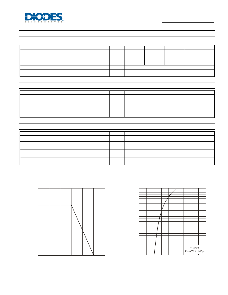
Fig. 1 Forward Current Derating Curve
T
°
3
4
0
Note 3
0.01
0.1
1.0
10
0
0.4
0.8
1.2
1.6
I,
I
N
S
T
A
N
T
A
N
E
O
U
S
F
O
R
WA
R
D
C
U
R
R
E
N
T
(A
)
F
V , INSTANTANEOUS FORWARD VOLTAGE (V)
Fig. 2 Typical Forward Characteristics
F