Dflf1800, New prod uc t, Maximum ratings – Diodes DFLF1800 User Manual
Page 2: Thermal characteristics, Electrical characteristics
DFLF1800
Document number: DS35083 Rev. 3 - 2
2 of 5
February 2014
© Diodes Incorporated
DFLF1800
PowerDI is a registered trademark of Diodes Incorporated.
NEW PROD
UC
T
Maximum Ratings
(@T
A
= +25°C, unless otherwise specified.)
Single phase, half wave, 60Hz, resistive or inductive load.
For capacitance load, derate current by 20%.
Characteristic Symbol
Value
Unit
Peak Repetitive Reverse Voltage
Working Peak Reverse Voltage
DC Blocking Voltage
V
RRM
V
RWM
V
R
800 V
Average Rectified Output Current (see figure 4)
I
O
1.0 A
Non-Repetitive Peak Forward Surge Current
8.3ms Single Half Sine-Wave Superimposed on Rated Load
I
FSM
25 A
Thermal Characteristics
Characteristic Symbol
Typ
Max
Unit
Thermal Resistance, Junction to Ambient Air (Note 5)
R
ΘJA
134
⎯
°C/W
Thermal Resistance, Junction to Soldering Point (Note 6)
R
ΘJS
⎯
6 °C/W
Operating and Storage Temperature Range
T
J,
T
STG
⎯
-65 to +150
°C
Electrical Characteristics
(@T
A
= +25°C, unless otherwise specified.)
Characteristic Symbol
Min
Typ
Max
Unit
Test
Conditions
Reverse Breakdown Voltage (Note 7)
V
(BR)R
800
⎯
⎯
V
I
R
= 10
μA
Forward Voltage Drop
V
F
⎯
⎯
1.35 V
I
F
= 1.0A, T
J
= +25
°C
Reverse Leakage Current
I
R
⎯
⎯
⎯
⎯
10
20
μA
V
R
= 800V, T
J
= +25
°C
V
R
= 800V, T
J
= +125
°C
Total Capacitance
C
T
⎯
7
⎯
pF
V
R
= 4.0V
DC
, f = 1MHz
Reverse Recovery Time
t
rr
⎯
⎯
500 ns
I
F
= 0.5A, I
R
= 1A, I
RR
= 0.25A
Notes:
5. Device mounted on 1" x 1", FR-4 PCB; 2 oz. Cu pad layout as shown on Diodes Inc. suggested pad layout document AP02001.pdf. T
A
= 25°C
6. Theoretical R
θJS
calculated from the top center of the die straight down to the PCB/cathode tab solder junction.
7.
Short duration test pulse used to minimize self-heating effect.
0
0.4
0.8
1.2
1.6
I,
IN
S
TA
N
TA
N
E
O
U
S
F
O
R
WA
R
D
C
U
R
R
E
N
T
(mA
)
F
1
10
100
1,000
10,000
0.1
V , INSTANTANEOUS FORWARD VOLTAGE (V)
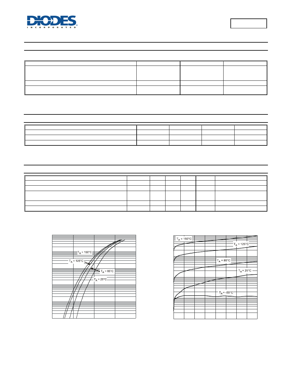
Figure 1 Typical Forward Characteristics
F
V , INSTANTANEOUS REVERSE VOLTAGE (V)
R
Figure 2 Typical Reverse Characteristics
I
, IN
S
TAN
TAN
E
O
U
S
R
EVE
R
SE
C
U
R
R
EN
T
(µ
A
)
R
0.001
0.01
0.1
1
10
0
100
200
300
400
500
600
700
800