New prod uc t, Maximum ratings, Thermal characteristics – Diodes DFLR1800 User Manual
Page 2: Electrical characteristics, Dflr1800
DFLR1800
Document number: DS35075 Rev. 2 - 2
2 of 4
December 2010
© Diodes Incorporated
DFLR1800
PowerDI is a registered trademark of Diodes Incorporated.
NEW PROD
UC
T
Maximum Ratings
@T
A
= 25°C unless otherwise specified
Single phase, half wave, 60Hz, resistive or inductive load.
For capacitance load, derate current by 20%.
Characteristic Symbol
Value
Unit
Peak Repetitive Reverse Voltage
Working Peak Reverse Voltage
DC Blocking Voltage
V
RRM
V
RWM
V
R
800 V
Average Rectified Output Current (see figure 4)
I
O
1.0 A
Non-Repetitive Peak Forward Surge Current
8.3ms Single Half Sine-Wave Superimposed on Rated Load
I
FSM
25 A
Thermal Characteristics
Characteristic Symbol
Typ
Max
Unit
Thermal Resistance, Junction to Ambient Air (Note 3)
R
θJA
134
⎯
°C/W
Thermal Resistance, Junction to Soldering Point (Note 4)
R
θJS
⎯
6 °C/W
Operating and Storage Temperature Range
T
J,
T
STG
⎯
-65 to +150
°C
Electrical Characteristics
@T
A
= 25°C unless otherwise specified
Characteristic Symbol
Value
Unit
Forward Voltage @ I
F
= 1.0A
V
FM
1.1 V
Peak Reverse Leakage Current @ T
A
= 25
°C
at Rated DC Blocking Voltage @ T
A
= 125
°C
I
RM
10
150
μA
Typical Total Capacitance (f = 1MHz, V
R
= 4.0VDC)
C
T
10 pF
Notes:
3. Device mounted on 1" x 1", FR-4 PCB; 2 oz. Cu pad layout as shown on Diodes Inc. suggested pad layout document AP02001.pdf. T
A
= 25°C
4. Theoretical R
θJS
calculated from the top center of the die straight down to the PCB/cathode tab solder junction.
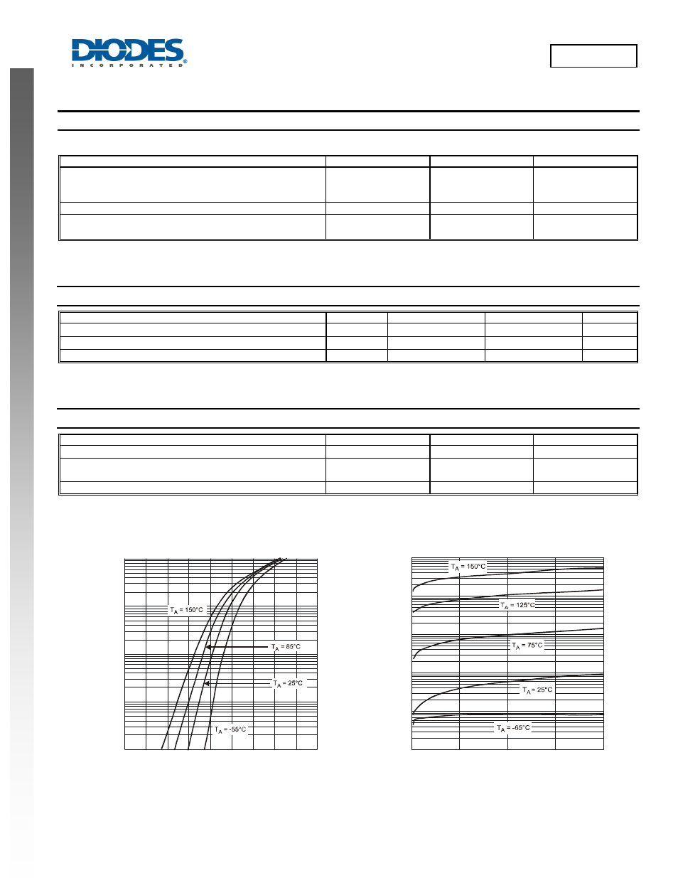
V , INSTANTANEOUS FORWARD VOLTAGE (V)
Fig. 1 Typical Forward Characteristics
F
I,
I
N
S
T
A
NT
A
N
E
O
U
S
F
O
R
W
A
R
D
C
U
R
R
E
NT
(m
A
)
F
0.2
0.4
0.6
0.8
1
1.2
1.4
1.6
1
10
100
1,000
10,000
0
1.8
0
0.0001
0.001
0.01
0.1
1
10
PERCENT OF RATED PEAK REVERSE VOLTAGE (%)
Fig. 2 Typical Reverse Characteristics
25
50
75
100
I
,
IN
ST
AN
T
A
NEOUS R
EVE
R
S
E
CU
RR
E
N
T
(
µ
A)
R