Diodes MBR3030PT - MBR3060PT User Manual
30a schottky barrier rectifier features, Maximum ratings and electrical characteristics, Mechanical data
DS23017 Rev. 8 - 2
1 of 3
MBR3030PT - MBR3060PT
www.diodes.com
ã
Diodes Incorporated
MBR3030PT - MBR3060PT
30A SCHOTTKY BARRIER RECTIFIER
Features
A
B
E
G
J
L
M
N
P
Q
K
S
M
H
R
D
C
Maximum Ratings and Electrical Characteristics
@ T
A
= 25
°C unless otherwise specified
·
Guard Ring Die Construction for
Transient Protection
·
Low Power Loss, High Efficiency
·
High Surge Capability
·
High Current Capability and Low Forward Voltage Drop
·
For Use in Low Voltage, High Frequency Inverters, Free
Wheeling, and Polarity Protection Applications
·
Lead Free Finish, RoHS Compliant (Note 4)
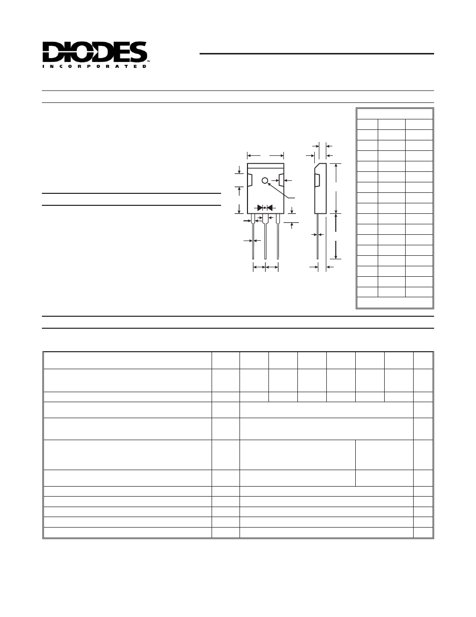
Mechanical Data
·
Case: TO-3P
·
Case Material: Molded Plastic. UL Flammability
Classification Rating 94V-0
·
Moisture Sensitivity: Level 1 per J-STD-020C
·
Terminals: Finish
¾ Bright Tin. Plated Leads Solderable
per MIL-STD-202, Method 208
·
Polarity: As Marked on Body
·
Ordering Information: See Last Page
·
Marking: Type Number
·
Weight: 5.6 grams (approximate)
Single phase, half wave, 60Hz, resistive or inductive load.
For capacitive load, derate current by 20%.
Characteristic
Symbol
MBR
3030PT
MBR
3035PT
MBR
3040PT
MBR
3045PT
MBR
3050PT
MBR
3060PT
Unit
Peak Repetitive Reverse Voltage
Working Peak Reverse Voltage
DC Blocking Voltage
V
RRM
V
RWM
V
R
30
35
40
45
50
60
V
RMS Reverse Voltage
V
R(RMS)
21
24.5
28
31.5
35
42
V
Average Rectified Output Current
@ T
C
= 125
°C
Total Device (See Fig. 1)
I
O
30
A
Non-Repetitive Peak Forward Surge Current
8.3ms Single half sine-wave superimposed on rated load
(JEDEC Method)
I
FSM
200
A
Forward Voltage Drop
@ I
F
= 20A, T
C
= 25
°C
per element (Note 3)
@ I
F
= 20A, T
C
= 125
°C
@ I
F
= 30A, T
C
= 25
°C
@ I
F
= 30A, T
C
= 125
°C
V
FM
¾
0.60
0.76
0.72
0.75
0.65
0.80
0.75
V
Peak Reverse Current
@ T
C
= 25
°C
at Rated DC Blocking Voltage, per element @ T
C
= 125
°C
I
RM
1.0
60
5.0
100
mA
Typical Total Capacitance
(Note 2)
C
T
500
pF
Typical Thermal Resistance Junction to Case
(Note 1)
R
qJc
1.4
°C/W
Voltage Rate of Change (Rated V
R
)
dV/dt
10,000
V/µs
Operating Temperature Range
T
j
-65 to +150
°C
Storage Temperature Range
T
STG
-65 to +175
°C
Notes: 1. Thermal resistance junction to case mounted on heatsink.
2. Measured at 1.0MHz and applied reverse voltage of 4.0V DC.
3. Pulse width
£300 ms, duty cycle £2%.
4.
RoHS revision 13.2.2003. Glass and High Temperature Solder Exemptions Applied, see
TO-3P
Dim
Min
Max
A
1.88
2.08
B
4.68
5.36
C
20.63
22.38
D
18.5
21.5
E
2.1
2.4
G
0.51
0.76
H
15.38
16.25
J
1.90
2.70
K
2.9
Ж
3.65
Ж
L
3.78
4.50
M
5.2
5.7
N
0.89
1.53
P
1.82
2.46
Q
2.92
3.23
R
11.70
12.84
S
¾
6.10
All Dimensions in mm