Dfls230l, Maximum ratings, Thermal characteristics – Diodes DFLS230L User Manual
Page 2: Electrical characteristics
DFLS230L
Document number: DS30515 Rev. 5 - 2
2 of 4
October 2010
© Diodes Incorporated
DFLS230L
PowerDI is a registered trademark of Diodes Incorporated.
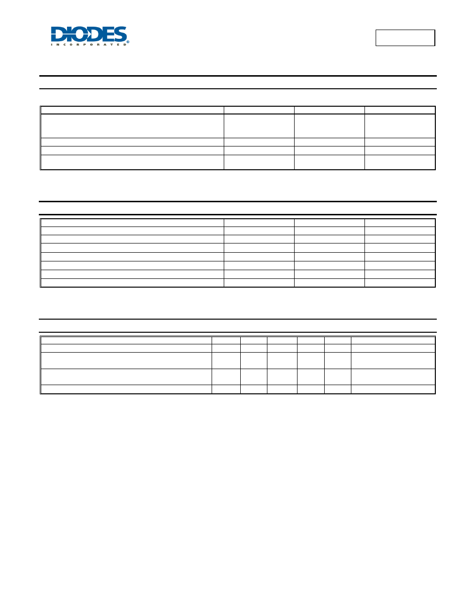
Maximum Ratings
@T
A
= 25°C unless otherwise specified
Single phase, half wave, 60Hz, resistive or inductive load.
For capacitance load, derate current by 20%.
Characteristic Symbol
Value
Unit
Peak Repetitive Reverse Voltage
Working Peak Reverse Voltage
DC Blocking Voltage
V
RRM
V
RWM
V
R
30 V
RMS Reverse Voltage
V
R(RMS)
21 V
Average Forward Current @ T
T
= 121°C
I
F(AV)
2.0 A
Non-Repetitive Peak Forward Surge Current 8.3ms
Single Half Sine-Wave Superimposed on Rated Load
I
FSM
33 A
Thermal Characteristics
Characteristic Symbol
Value
Unit
Power Dissipation (Note 3)
P
D
1.67 W
Power Dissipation (Note 4)
P
D
556 mW
Thermal Resistance Junction to Ambient (Note 3)
R
θJA
60
°C/W
Thermal Resistance Junction to Ambient (Note 4)
R
θJA
180
°C/W
Thermal Resistance Junction to Soldering (Note 5)
R
θJS
10
°C/W
Operating Temperature Range
T
J
-40 to +125
°C
Storage Temperature Range
T
STG
-40 to +150
°C
Electrical Characteristics
@T
A
= 25°C unless otherwise specified
Characteristic Symbol
Min
Typ
Max
Unit
Test
Condition
Reverse Breakdown Voltage (Note 6)
V
(BR)R
30
⎯
⎯
V
I
R
= 1.0mA
Forward Voltage
V
F
⎯
⎯
0.310
0.375
⎯
0.420
V
I
F
= 1.0A
I
F
= 2.0A
Leakage Current (Note 6)
I
R
⎯
⎯
0.260
⎯
⎯
1.0
mA
V
R
= 5V, T
A
= 25
°C
V
R
= 30V, T
A
= 25
°C
Total Capacitance
C
T
⎯
76
⎯
pF
V
R
= 10V, f = 1.0MHz
Notes:
3. Part mounted on 2"x2" GETEK board with 1"x1" copper pad, 25% anode, 75% cathode. T
A
= 25°C.
4. Part mounted on FR-4 board with recommended pad layout, which can be found on our websit5. Theoretical R
θJS
calculated from the top center of the die straight down to the PCB/cathode tab solder junction.
6. Short duration pulse test used to minimize self-heating effect.