Diodes DFLS240L User Manual
Dfls240l, Features, Mechanical data
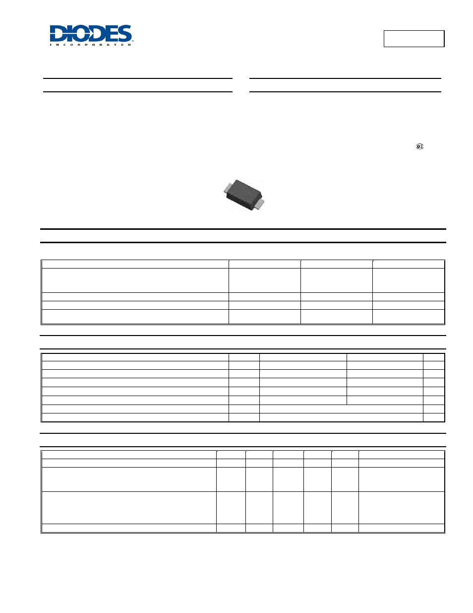
DFLS240L
Document number: DS30516 Rev. 8 - 2
1 of 4
www.diodes.com
November 2009
© Diodes Incorporated
DFLS240L
PowerDI is a registered trademark of Diodes Incorporated.
2.0A LOW VF SCHOTTKY BARRIER RECTIFIER
PowerDI
®
123
Features
•
Guard Ring Die Construction for Transient Protection
•
Low Power Loss, High Efficiency
•
High Surge Capability
•
High Current Capability and Low Forward Voltage Drop
•
Lead Free Finish, RoHS Compliant (Note 4)
•
"Green" Molding Compound (No Br, Sb)
•
Qualified to AEC-Q101 Standards for High Reliability
Mechanical Data
• Case:
PowerDI
®
123
•
Case Material: Molded Plastic, "Green" Molding Compound.
UL Flammability Classification Rating 94V-0
•
Moisture Sensitivity: Level 1 per J-STD-020
•
Terminal Connections: Cathode Band
•
Terminals: Finish – Matte Tin Annealed Over Copper
leadframe. Solderable per MIL-STD-202, Method 208
•
Marking Information: See Page 2
•
Ordering Information: See Page 2
•
Weight: 0.01 grams (approximate)
Maximum Ratings
@T
A
= 25°C unless otherwise specified
Single phase, half wave, 60Hz, resistive or inductive load.
For capacitance load, derate current by 20%.
Characteristic
Symbol
Value
Unit
Peak Repetitive Reverse Voltage
Working Peak Reverse Voltage
DC Blocking Voltage
V
RRM
V
RWM
V
R
40
V
RMS Reverse Voltage
V
R(RMS)
28
V
Average Forward Current
I
F(AV)
2.0
A
Non-Repetitive Peak Forward Surge Current 8.3ms
Single Half Sine-Wave Superimposed on Rated Load
I
FSM
50
A
Thermal Characteristics
Characteristic
Symbol
Typ
Max
Unit
Power Dissipation (Note 1)
P
D
⎯
1.67 W
Power Dissipation (Note 2)
P
D
⎯
556
mW
Thermal Resistance Junction to Ambient (Note 1)
R
θJA
60
⎯
°C/W
Thermal Resistance Junction to Ambient (Note 2)
R
θJA
180
⎯
°C/W
Thermal Resistance Junction to Soldering (Note 3)
R
θJS
⎯
5
°C/W
Operating Temperature Range (See figure 4)
T
J
-55 to +125
°C
Storage Temperature Range
T
STG
-55 to +150
°C
Electrical Characteristics
@T
A
= 25°C unless otherwise specified
Characteristic
Symbol
Min
Typ
Max
Unit
Test Condition
Reverse Breakdown Voltage (Note 5)
V
(BR)R
40
⎯
⎯
V
I
R
= 500
μA
Forward Voltage
V
F
⎯
⎯
⎯
0.4
0.45
0.50
0.45
0.50
0.65
V
I
F
= 1.0A
I
F
= 2.0A
I
F
= 3.0A
Leakage Current (Note 5)
I
R
⎯
⎯
⎯
⎯
⎯
⎯
⎯
⎯
0.1
10
0.05
5
mA
V
R
= 40V
V
R
= 40V, T
J
= 85
°C
V
R
= 20V
V
R
= 20V, T
J
= 85
°C
Total Capacitance
C
T
⎯
90
⎯
pF
V
R
= 10V, f = 1.0MHz
Notes:
1. Part mounted on 50.8mm X 50.8mm GETEK board with 25.4mm X 25.4mm copper pad, 25% anode, 75% cathode.
2. Part mounted on FR-4 board with 1.8mm X 2.5mm cathode and 1.8mm X 1.2mm anode, 1 oz. copper pads.
3. Theoretical R
θJS
calculated from the top center of the die straight down to the PCB cathode tab solder junction.
4. EU Directive 2002/95/EC (RoHS). All applicable RoHS exemptions applied. Please visit our website at
5. Short duration pulse test used to minimize self-heating effect.
Top View