Marking information, Package outline dimensions, B130law – Diodes B130LAW User Manual
Page 3: Ordering information
B130LAW
0
2.5
5.0
7.5
10
12.5
1
10
I,
100
P
E
AK
F
O
R
WA
R
D S
U
R
G
E
C
U
R
R
E
N
T
(A
)
FS
M
NUMBER OF CYCLES AT 60 Hz
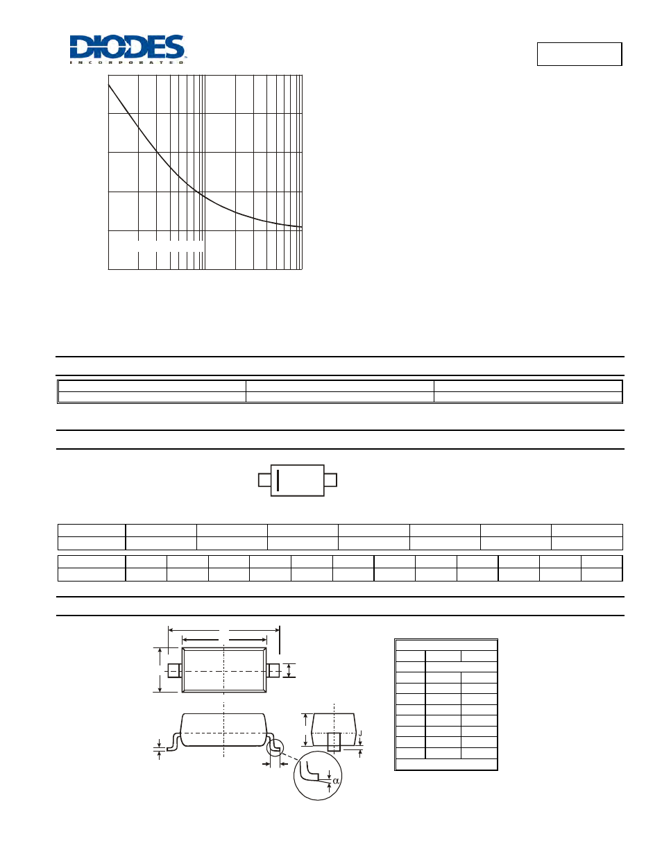
Fig. 7 Maximum Non-Repetitive Peak Forward Surge Current
8.3ms Single Half Sine-Wave
Notes:
5. Device mounted on GETEK substrate, 2”x2”, 2 oz. copper, double-sided, cathode pad dimensions 0.75” x 1.0”, anode pad dimensions 0.25” x 1.0”.
6. Device mounted on FR-4 substrate, 2”x2”, 2 oz. copper, single-sided, pad layout as per Diodes Inc. suggested pad layout document AP02001 which
can be found on our website at http://www.diodes.com/datasheets/ap02001.pdf.
7. R
θJA
estimated to be approximately 220 °C/W.
Ordering Information
(Note 8)
Part Number
Case
Packaging
B130LAW-7-F
SOD-123
3000/Tape & Reel
Notes:
8. For packaging details, go to our website at
Marking Information
SX = Product Type Marking Code
YM = Date Code Marking
Y = Year ex: T = 2006
M = Month (ex: 9 = September)
SX
YM
Date Code Key
B130LAW
Document number: DS30308 Rev. 9 - 2
3 of 4
www.diodes.com
June 2008
© Diodes Incorporated
Year
2006
2007
2008
2009
2010
2011
2012
Code
T
U
V
W
X
Y
Z
Month
Jan
Feb
Mar
Apr
May
Jun
Jul
Aug
Sep
Oct
Nov
Dec
Code 1 2 3 4 5 6 7 8 9 O N D
Package Outline Dimensions
K
L
M
C
H
B
A
SOD-123
Dim
Min Max
A
0.55 Typ
B
1.40 1.70
C
3.55 3.85
H
2.55 2.85
J
0.00 0.10
K
1.00 1.35
L
0.25 0.40
M
0.10 0.15
0 8°
α
All Dimensions in mm