Single 2 input exclusive or gate, New prod uc t electrical characteristics – Diodes 74LVCE1G86 User Manual
Page 5
74LVCE1G86
SINGLE 2 INPUT EXCLUSIVE OR GATE
74LVCE1G86
Document number: DS32215 Rev. 2 - 2
5 of 14
December 2010
© Diodes Incorporated
NEW PROD
UC
T
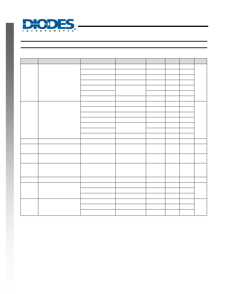
Electrical Characteristics
(All typical values are at Vcc = 3.3V, T
A
= 25°C)
Over recommended free-air temperature range (unless otherwise noted)
Symbol
Parameter
Test Conditions
Vcc
Min
Typ.
Max
Unit
V
OH
High Level Output
Voltage
I
OH
= -100
μA
1.4 V to 5.5V
V
CC
– 0.1
V
I
OH
= -3mA
1.4 V
1.05
I
OH
= -4mA
1.65 V
1.2
I
OH
= -8mA
2.3V
1.9
I
OH
= -16mA
3 V
2.4
I
OH
= -24mA
2.3
I
OH
= -32mA
4.5 V
3.8
V
OL
High-level Input Voltage
I
OL
= 100
μA
1.4 V to 5.5V
0.1
V
I
OL
= 3mA
1.4 V
.4
I
OL
= 4mA
1.65 V
0.45
I
OL
= 8mA
2.3V
0.3
I
OL
= 16mA
3 V
0.4
I
OL
= 24mA
0.55
I
OL
= 32mA
4.5
0.55
I
I
Input Current
V
I
= 5.5 V or GND
0 to 5.5 V
± 5
μA
I
OFF
Power Down Leakage
Current
V
I
or V
O
= 5.5V
0
± 10
μA
I
CC
Supply
Current
V
I
= 5.5V of GND
I
O
=0
1.4 V to 5.5V
10
μA
ΔI
CC
Additional Supply
Current
One input at V
CC
–
0.6 V Other inputs
at V
CC
or GND
3 V to 5.5V
500
μA
C
i
Input
Capacitance
V
i
= V
CC
– or GND
3.3
3.5
pF
θ
JA
Thermal Resistance
Junction-to-Ambient
SOT25 (Note
5)
204
o
C/W
SOT353
(Note 5)
371
DFN1410 (Note
5)
430
θ
JC
Thermal Resistance
Junction-to-Case
SOT25 (Note
5)
52
o
C/W
SOT353 (Note
5)
143
DFN1410
(Note 5)
190
Note: 5. Test condition for SOT25, SOT353, and DFN1410: Device mounted on FR-4 substrate PC board, 2oz copper, with minimum
recommended pad layout.