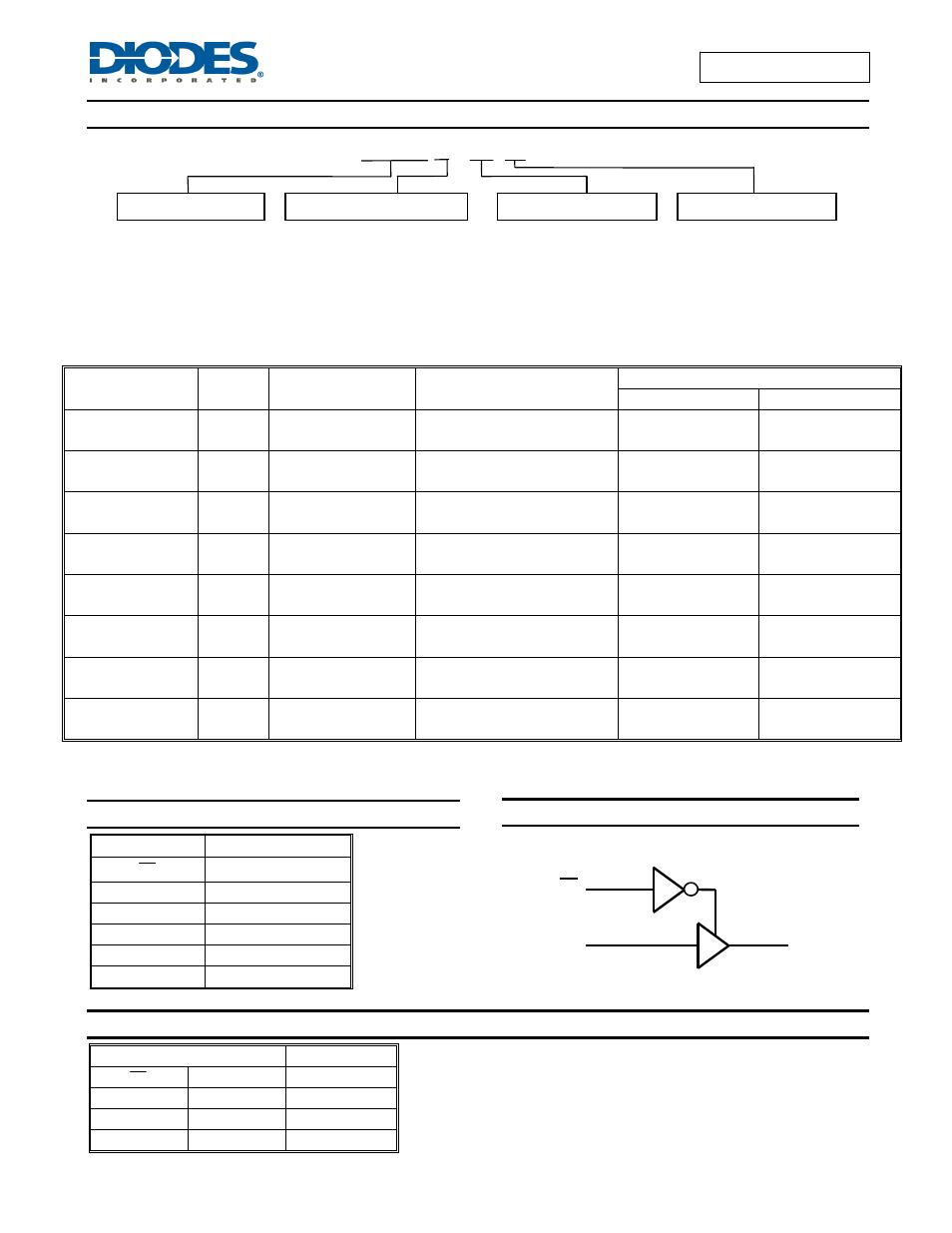
Pin descriptions, Logic diagram, Function table – Diodes 74LVC1G125 User Manual
Page 2
74LVC1G125
Document number: DS32202 Rev. 7 - 2
2 of 15
March 2014
© Diodes Incorporated
74LVC1G125
Ordering Information
74 LVC1G 125 XXX -7
Logic Device
Function Package
Packing
74 : Logic Prefix
125: 3-State Buffer
W5 : SOT25
-7 : 7” Tape & Reel
LVC : 1.65 to 5.5 V
OE active low
SE : SOT353
Logic Family
Z : SOT553
1G : One Gate
FS3 : X2-DFN0808-4
FW5 :
X1-DFN1010-6
FW4
:X2-DFN1010-6
FX4 : X2- DFN1409-6
FZ4 : X2- DFN1410-6
Notes:
4. Pad layout as shown on Diodes Inc. suggested pad layout document AP02001, which can be found on our website at
5. The taping orientation is located on our website at
Pin Descriptions
Pin Name
Description
OE
Output Enable
A Data
Input
GND Ground
Y Data
Output
V
CC
Supply Voltage
NC No
Connection
Logic Diagram
Function Table
Inputs Output
OE
A Y
L H H
L L L
H X Z
Device
Package
Code
Package
(Notes 4, 5)
Package
Size
7” Tape and Reel
Quantity
Part Number Suffix
74LVC1G125W5-7
W5
SOT25
3.0mm X 2.8mm X 1.2mm
0.95mm lead pitch
3000/Tape & Reel
-7
74LVC1G125SE-7
SE
SOT353
2.0mm X 2.0mm X 1.1mm
0.65mm lead pitch
3000/Tape & Reel
-7
74LVC1G125Z-7 Z SOT553
1.6mm X 1.6 mm X 0.62mm
0.5mm lead pitch
4000/Tape & Reel
-7
74LVC1G125FS3-7
FS3
X2-DFN0808-4
0.9mm X 0.9 mm X 0.35mm
0.5mm pad pitch (diamond)
5000/Tape & Reel
-7
74LVC1G125FW5-7
(Future Product)
FW5
X1-DFN1010-6
(Future Product)
1.0mm X 1.0mm X 0.5mm
0.35mm pad pitch
5000/Tape & Reel
-7
74LVC1G125FW4-7 FW4 X2-DFN1010-6
1.0mm X 1.0mm X 0.4mm
0.35mm pad pitch
5000/Tape & Reel
-7
74LVC1G125FX4-7 FX4
X2-DFN1409-6
(Chip scale alternative)
1.4mm X 0.9mm X 0.4mm
0.5mm pad pitch
5000/Tape & Reel
-7
74LVC1G125FZ4-7
FZ4 X2-DFN1410-6
1.4mm X 1.0mm X 0.4mm
0.5mm pad pitch
5000/Tape & Reel
-7
1
2
4
A
OE
Y