Diodes 74LVC1G07 User Manual
Description, Features, Pin assignments
74LVC1G07
Document number: DS32274 Rev. 7 - 2
1 of 14
March 2014
© Diodes Incorporated
74LVC1G07
SINGLE BUFFER/DRIVER WITH OPEN DRAIN OUTPUT
Description
The 74LVC1G07 is a single buffer gate with an open drain output.
The device is designed for operation with a power supply range of
1.65V to 5.5V. The input is tolerant to 5.5V allowing this device to be
used in a mixed voltage environment. The device is fully specified
for partial power down applications using I
OFF
. The I
OFF
circuitry
disables the output preventing damaging current backflow when the
device is powered down. The open-drain output can be connected to
other open drain outputs to implement active-low wired-OR or active-
high wired-AND functions. The maximum sink current is 32 mA.
Features
Wide Supply Voltage Range from 1.65 to 5.5V
24mA Sink Current at 3.3V
CMOS low power consumption
I
OFF
Supports Partial-Power-Down Mode Operation
Inputs accept up to 5.5V
ESD Protection Tested per JESD 22
o
Exceeds 200-V Machine Model (A115)
o
Exceeds 2000-V Human Body Model (A114)
o
Exceeds 1000-V Charged Device Model (C101)
Latch-Up Exceeds 100mA per JESD 78, Class I
Range of Package Options
Totally Lead-Free & Fully RoHS Compliant (Notes 1 & 2)
Halogen and Antimony Free. “Green” Device (Note 3)
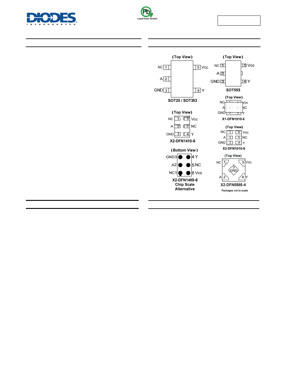
Pin Assignments
Applications
Voltage Level Shifting
General Purpose Logic
Power Down Signal Isolation
Wide array of products such as:
o
PCs, networking, notebooks, netbooks, PDAs
o
Tablet Computers, E-readers
o
Computer peripherals, hard drives, CD/DVD ROM
o
TV, DVD, DVR, set top box
o
Cell Phones, Personal Navigation / GPS
o
MP3 players ,Cameras, Video Recorders
Notes:
1. No purposely added lead. Fully EU Directive 2002/95/EC (RoHS) & 2011/65/EU (RoHS 2) compliant.
2. Se information about Diodes Incorporated’s definitions of Halogen- and Antimony-free, "Green" and Lead-free.
3. Halogen- and Antimony-free "Green” products are defined as those which contain <900ppm bromine, <900ppm chlorine (<1500ppm total Br + Cl)
and <1000ppm antimony compounds.
Future
Product