Ordering information, Pin descriptions, Logic diagram – Diodes 74LVC1G00 User Manual
Page 2: Function table
74LVC1G00
Document number: DS32196 Rev. 7 - 2
2 of 15
www.diodes.com
March 2014
© Diodes Incorporated
NEW PROD
UC
T
74LVC1G00
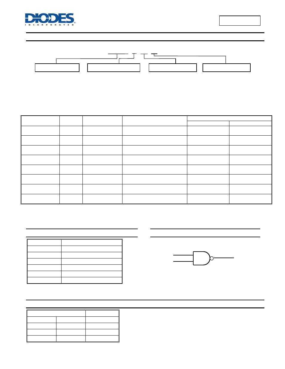
Ordering Information
74 LVC1G 00 XXX -7
Logic Device
Function
Package
Packing
74 : Logic Prefix
00 :
2-Input
W5 : SOT25
-7 : 7” Tape & Reel
LVC : 1.65 to 5.5 V
NAND Gate
SE : SOT353
Logic Family
Z : SOT553
1G : One Gate
FS3 : X2-DFN0808-4
FW5 : X1-DFN1010-6
FW4
:X2-DFN1010-6
FX4 : X2- DFN1409-6
FZ4 : X2- DFN1410-6
Notes: 4. Pad layout as shown on Diodes Inc. suggested pad layout document AP02001, which can be found on our website at
http://www.diodes.com/datasheets/ap02001.pdf.
5. The taping orientation is located on our website at http://www.diodes.com/datasheets/ap02007.pdf
Pin Descriptions
Pin Name
Description
A Data
Input
B Data
Input
GND Ground
Y Data
Output
V
CC
Supply Voltage
NC No
Connection
Logic Diagram
Function Table
Inputs Output
A B Y
H H L
L X H
X L H
Device
Package
Code
Package
(Notes 4, 5)
Package
Size
7” Tape and Reel
Quantity
Part Number Suffix
74LVC1G00W5-7
W5
SOT25
3.0mm X 2.8mm X 1.2mm
0.95 mm lead pitch
3000/Tape & Reel
-7
74LVC1G00SE-7
SE
SOT353
2.0mm X 2.0mm X 1.1mm
0.65 mm lead pitch
3000/Tape & Reel
-7
74LVC1G00Z-7 Z SOT553
1.6mm X 1.6 mm X 0.62mm
0.5 mm lead pitch
4000/Tape & Reel
-7
74LVC1G00FS3-7
FS3
X2-DFN0808-4
0.9mm X 0.9 mm X 0.35mm
0.5 mm pad pitch (diamond)
5000/Tape & Reel
-7
74LVC1G00FW5-7
(Future Product)
FW5
X1-DFN1010-6
(Future Product)
1.0mm X 1.0mm X 0.5mm
0.35 mm pad pitch
5000/Tape & Reel
-7
74LVC1G00FW4-7 FW4 X2-DFN1010-6
1.0mm X 1.0mm X 0.4mm
0.35 mm pad pitch
5000/Tape & Reel
-7
74LVC1G00FX4-7 FX4
X2-DFN1409-6
Chip scale alternative
1.4mm X 0.9mm X 0.4mm
0.5 mm pad pitch
5000/Tape & Reel
-7
74LVC1G00FZ4-7
FZ4 X2-DFN1410-6
1.4mm X 1.0mm X 0.4mm
0.5 mm pad pitch
5000/Tape & Reel
-7
1
A
2
4
Y
B