Single inverter gate, New prod uc t electrical characteristics, Switching characteristics – Diodes 74AHCT1G04 User Manual
Page 4: Operating characteristics
74AHCT1G04
SINGLE INVERTER GATE
74AHCT1G04
Document number: DS35181 Rev. 1 - 2
4 of 8
May 2011
© Diodes Incorporated
NEW PROD
UC
T
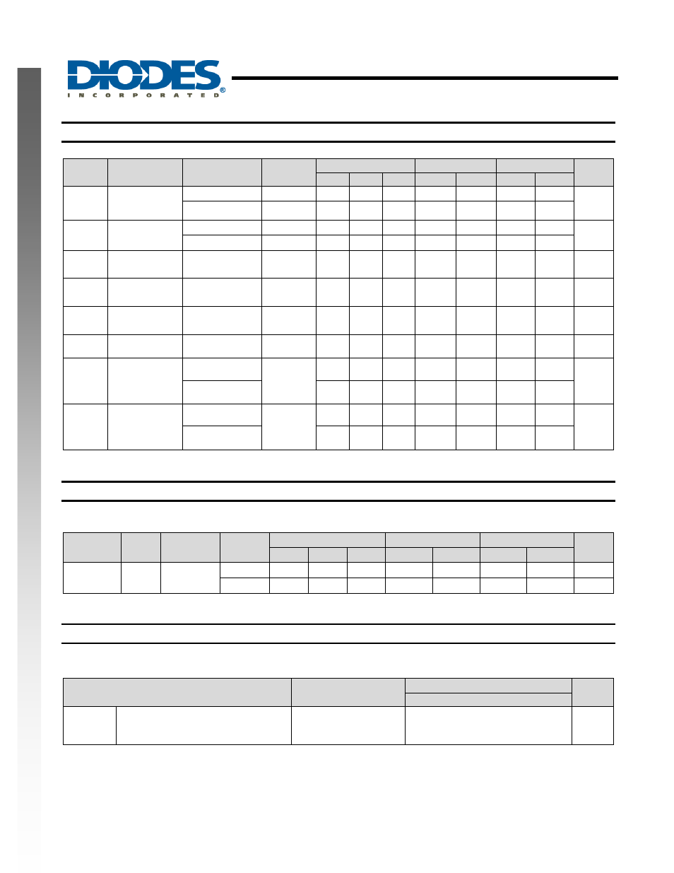
Electrical Characteristics
Symbol
Parameter
Test
Conditions
V
CC
25ºC
-40ºC to 85ºC
-40ºC to 125ºC
Unit
Min
Typ.
Max
Min
Max
Min
Max
V
OH
High Level
Output Voltage
I
OH
= -50
μA
4.5V 4.4
4.5 4.4 4.4
V
I
OH
= -8mA
4.5V 3.94 3.8
3.70
V
OL
Low Level
Output Voltage
I
OL
= 50
μA
4.5V 0
0.1 0.1
0.1
V
I
OL
= 8mA
4.5V
0.36
0.44
0.55
I
I
Input Current
V
I
= 5.5V or
GND
0 to 5.5V
± 0.1
± 1
± 2
μA
I
CC
Supply Current
V
I
= 5.5V or
GND I
O
=0
5.5V 1 10
40
μA
C
i
Input
Capacitance
V
I
= V
CC
– or
GND
5.5V
2.0
10 10
10 pF
ΔI
CC
Additional
Supply Current
Input at 3.4 V
5.5V
1.35
1.5
mA
θ
JA
Thermal
Resistance
Junction-to-
Ambient
SOT25
(Note 4)
204
o
C/W
SOT353
371
θ
JC
Thermal
Resistance
Junction-to-
Case
SOT25
(Note 4)
52
o
C/W
SOT353
143
Note: 4. Test conditions for SOT25, and SOT353: Device mounted on FR-4 substrate PC board, 2oz copper, with minimum recommended pad layout.
Switching Characteristics
V
CC
= 5V ± 0.5V
(see Figure 1)
Parameter
From
(Input)
TO
(OUTPUT)
25ºC
-40ºC to 85ºC
-40ºC to 125ºC
Unit
Min
Typ.
Max
Min
Max
Min
Max
t
pd
A
Y
C
L
=15pF
0.6 3.4 6.7 0.6 7.5 0.6 8.5 ns
C
L
=50pF
0.6 4.9 7.7 0.6 8.5 0.6 10.05 ns
Operating Characteristics
T
A
= 25 ºC
Parameter
Test
Conditions
V
CC
= 5 V
Unit
Typ.
C
pd
Power dissipation capacitance
f = 1 MHz
No Load
15
pF