74lvc14a, Switching characteristics, Operating characteristics – Diodes 74LVC14A User Manual
Page 5: Package characteristics
74LVC14A
Document number: DS35262 Rev. 3 - 2
5 of 10
July 2012
© Diodes Incorporated
74LVC14A
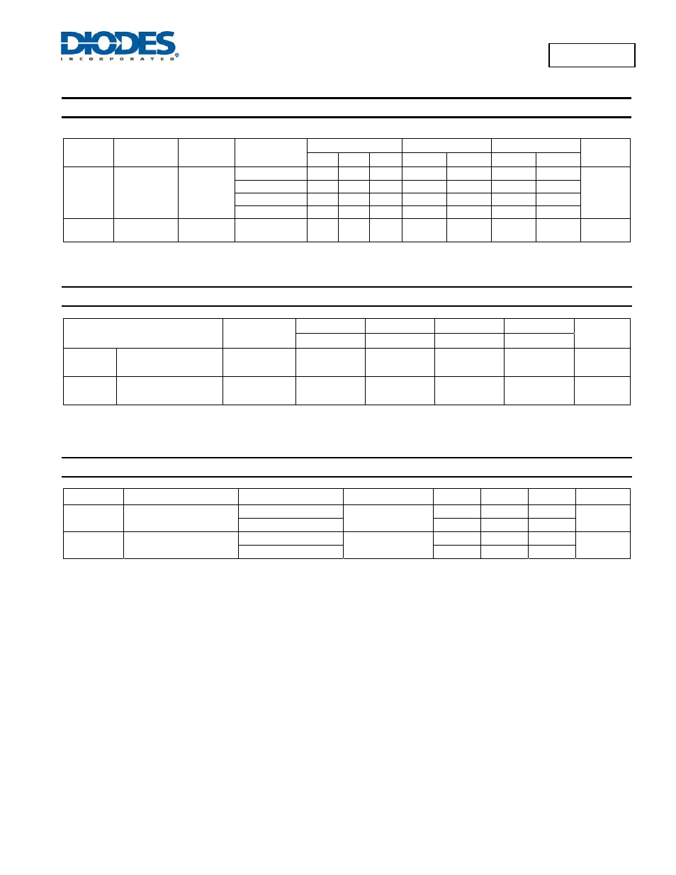
Switching Characteristics
Symbol
Parameter
Test
Conditions
V
CC
T
A
= +25°C
-40°C to +85°C
-40°C to +125°C
Unit
Min
Typ
Max
Min Max Min Max
t
PD
Propagation
Delay A
N
to Y
N
Figure 1
1.65V
to1.95V
0.5
4.1
8.9
0.5 8.9 0.5 9.5
ns
2.3V
to
2.7V
0.5
3.6
7.0
0.5 7.5 0.5 9.0
2.7V 0.5
3.0
5.3
0.5 5.5 0.5 7.0
3V
to
3.6V
0.5
2.5
4.8
0.5 4.8 0.5 6.0
t
SK(0)
Output Skew
Time
3V to 3.6V
1.0
1.5
ns
Operating Characteristics
(@T
A
= +25°C, unless otherwise specified.)
Parameter
Test
Conditions
V
CC
= 1.8V
V
CC
= 2.5V
V
CC
= 3.3V
V
CC
= 5V
Unit
Typ
Typ
Typ
Typ
C
pd
Power dissipation
capacitance per gate
f
=
10MHz
7.0 7.5 8.0 8.6
pF
C
I
Input Capacitance
V
i
= V
CC
– or
GND
4 4 4 4
pF
Package Characteristics
Symbol
Parameter
Test Conditions
V
CC
Min Typ Max Unit
θ
JA
Thermal Resistance
Junction-to-Ambient
SO-14
(Note 6)
TBD
o
C/W
TSSOP-14
159
θ
JC
Thermal Resistance
Junction-to-Case
SO-14
(Note 6)
TBD
o
C/W
TSSOP-14
25
Note:
6. Test condition for SO-14 and TSSOP-14: Device mounted on FR-4 substrate PC board, 2oz copper, with minimum recommended pad layout.