Absolute maximum ratings, Recommended operating conditions, Electrical characteristics – Diodes 74HCT126 User Manual
Page 3
74HCT126
Document number: DS35337 Rev. 3 - 2
3 of 8
January 2013
© Diodes Incorporated
74HCT126
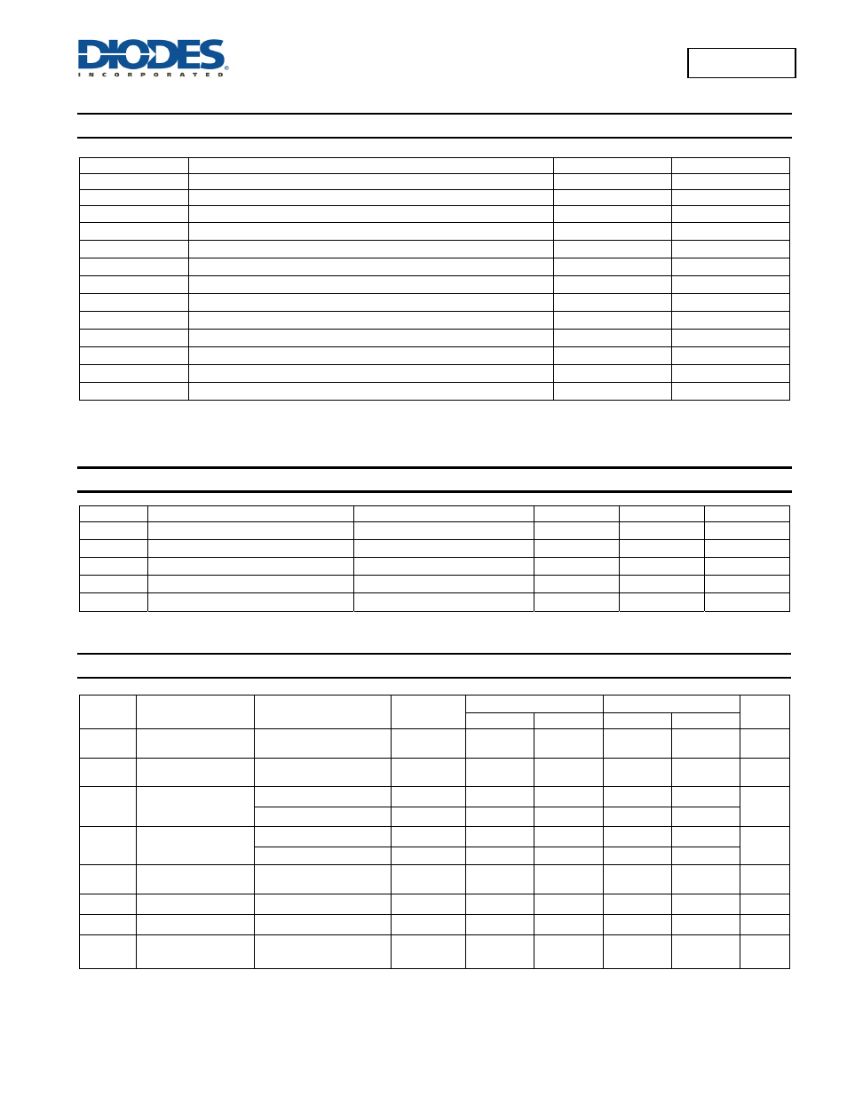
Absolute Maximum Ratings
(Note 4) (@T
A
= +25°C, unless otherwise specified.)
Symbol
Description
Rating
Unit
ESD HBM
Human Body Model ESD Protection
2
KV
ESD CDM
Charged Device Model ESD Protection
1
KV
ESD MM
Machine Model ESD Protection
200
V
V
CC
Supply Voltage Range
-0.5 to +7.0
V
V
I
Input Voltage Range (Note 5)
-0.5 to +7.0
V
I
IK
Input Clamp Current V
I
< -0.5V or Vi > V
CC
+0.5V
±20 mA
I
OK
Output Clamp Current V
O
< -0.5V or V
O
> V
CC
+0.5V
±20
mA
I
O
Continuous Output Current -0.5V < V
O
V
CC
+0.5V
+/-25 mA
I
CC
Continuous Current Through V
CC
50 mA
I
GND
Continuous Current Through GND
-50
mA
T
J
Operating Junction Temperature
-40 to +150
°C
T
STG
Storage Temperature
-65 to +150
°C
P
TOT
Total Power Dissipation
500
mW
Notes:
4. Stresses beyond the absolute maximum may result in immediate failure or reduced reliability. These are stress values and device operation should
be within recommend values.
5. Input Voltage cannot exceed V
CC
to the extent the Maximum clamp current is exceeded.
Recommended Operating Conditions
(Note 6) (@T
A
= +25°C, unless otherwise specified.)
Symbol Parameter
Conditions Min
Max
Unit
V
CC
Supply Voltage
4.5 5.5 V
V
I
Input Voltage
0
V
CC
V
V
O
Output Voltage
0
V
CC
V
Δt/ΔV
Input Transition Rise or Fall Rate
V
CC
= 4.5V to 5.5V
500
ns/V
T
A
Operating Free-Air Temperature
-40 +125 °C
Note: 6. Unused inputs should be held at V
CC
or Ground.
Electrical Characteristics
(@T
A
= +25°C, unless otherwise specified.)
Symbol Parameter
Test
Conditions
V
CC
T
A
= -40°C to +85°C
T
A
= -40°C to +125°C
Unit
Min Max Min Max
V
IH
High-level Input
Voltage
4.5V to 5.5V
2.0
2.0
V
V
IL
Low-level Input
Voltage
4.5V to 5.5V
0.8
0.8
V
V
OH
High-level Output
Voltage
I
OH
= -20μA
4.5V
4.4 4.4
V
I
OH
= -4mA
4.5V
3.84 3.70
V
OL
Low-level Output
Voltage
I
OL
= 20μA
4.5V 0.1 0.1
V
I
OL
= 4.0mA
4.5V 0.33 0.4
I
OZ
Z State Leakage
Current
V
O
= 0 to 5.5V
5.5V ±
5.0 ±
10
μA
I
I
Input Current
V
I
= GND to 6.0V
6.0V ±
1 ±
1
μA
I
CC
Supply Current
V
I
= GND or V
CC
, I
O
= 0
6.0V 20 40
μA
ΔI
CC
Additional Supply
Current
One Input at V
CC
-2.1V
Other Pins at V
CC
or GND
4.5V
to
5.5V
675 735
μA