74hc05 new prod uc t, Switching characteristics, Operating characteristics – Diodes 74HC05 User Manual
Page 4: Parameter measurement information
74HC05
Document number: DS35321 Rev. 3 - 2
4 of 7
January 2013
© Diodes Incorporated
74HC05
NEW PROD
UC
T
Switching Characteristics
Symbol
Parameter
Test
Conditions
V
CC
T
A
= +25°C
-40°C to +85°C
-40°C to +125°C
Unit
Min Typ Max
Max Max
t
PD
Propagation
Delay A
N
to Y
N
Figure 1
C
L
= 50 pF
2.0V —
25
90 115
125
ns
4.5V
—
9
18
23
27
6.0V —
7
15 20
23
t
t
Transition time
Figure 1
C
L
= 50 pF
2.0V —
19
75 95
110
ns
4.5V
—
7
15
19
22
6.0V —
6
13 16
19
Operating Characteristics
(@T
A
= +25°C, unless otherwise specified.)
Parameter Test
Conditions
V
CC
= 6V
Unit
Typ
C
pd
Power dissipation
capacitance per gate
f = 1 MHz
22
pF
C
I
Input Capacitance
V
I
= V
CC
– or GND
4 pF
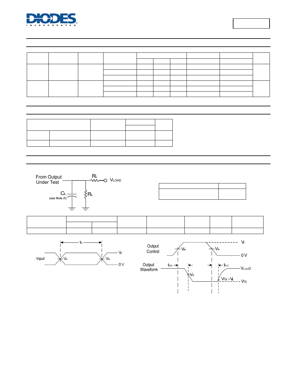
Parameter Measurement Information
V
CC
Inputs
V
M
V
LOAD
C
L
R
L
V∆
V
I
t
r
/t
f
2.0V to 6.0V
V
CC
≤6ns
V
CC
/2
2 X V
CC
50 pF
2 KΩ
10% of Vcc
Voltage Waveform
Pulse Duration
Voltage Waveform
Propagation Delay Times
Notes:
A. Includes test lead and test apparatus capacitance.
B. All pulses are supplied at pulse repetition rate ≤ 1 MHz.
C.The inputs are measured one at a time with one transition per measurement.
D. For the open drain device t
PLZ
and t
PZL
are the same as t
PD.
E.
t
PZL
is measured at V
M
.
F.
t
PLZ
is measured at V
OL
+V
∆.
D. A Thevenin equivalent load may be used in place of V
CC
X 2 and resistor divider.
Figure 1 Load Circuit and Voltage Waveforms
TEST Condition
t
PLZ
(see Notes D and E)
t
PZL
(see Notes D and F)
Vload
Vload