Functional description and timing diagram – Diodes 74AHC595 User Manual
Page 3
74AHC595
Document number: DS35486 Rev. 3 - 2
3 of 10
June 2013
© Diodes Incorporated
74AHC595
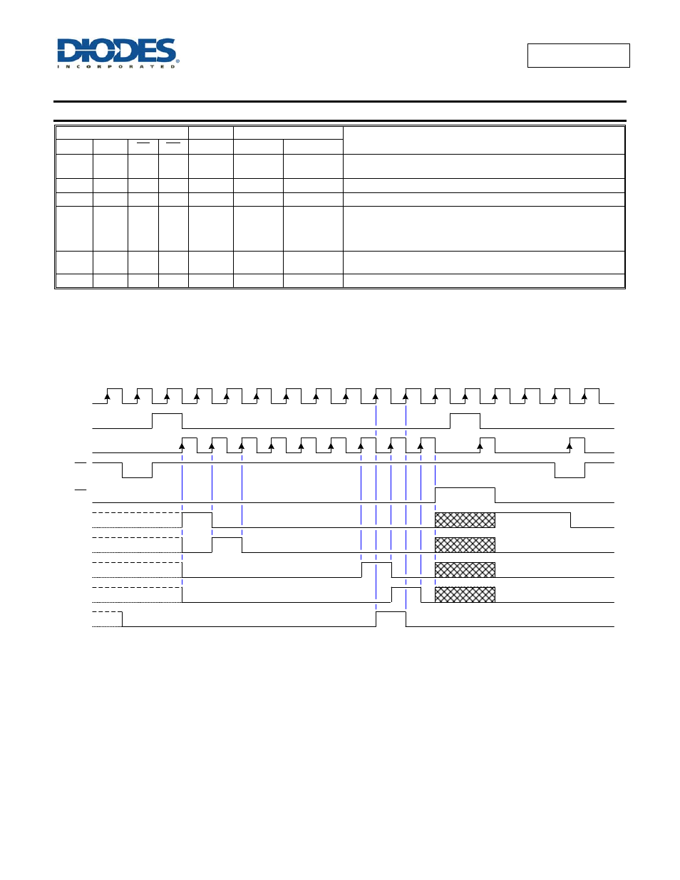
Functional Description and Timing Diagram
Control Input
Output
Function
SHCP STCP OE MR DS Q7S
Qn
X X L
L
L NC
Low-level asserted on MR clears shift register.
Storage register is unchanged
X
L L
L L
Empty shift register transferred to storage register
X X H
L
L Z
Shift register remains clear;: All Q ouputs in Z state.
X L H
Q6S NC
HIGH is shifted into first stage of Shift Register Contents of each
register shifted to next register
The content of Q6S has been shifted to Q7S and now appears on
device pin Q7S
X
L H
NC QnS
Contents of shift register copied to storage register. With output now
in active state the storage resister contents appear on Q outputs.
L H
Q6S QnS
H=HIGH voltage state
L=LOW voltage state
=LOW to HIGH transition
X= don’t care – high or low (not floating)
NC= No change
Z= high-impedance state
SHCP
DS
STCP
MR
OE
Q0
Q1
Q6
Q7
Q7S
Z-state
Z-state
Z-state
Z-state