Data sheet, Pin description – Diodes AP389X User Manual
Page 5
Data Sheet
Enhanced Multi-touch Capacitive Touch Screen Controller AP389X
Apr. 2013 Rev. 1. 0 BCD Semiconductor Manufacturing Limited
5
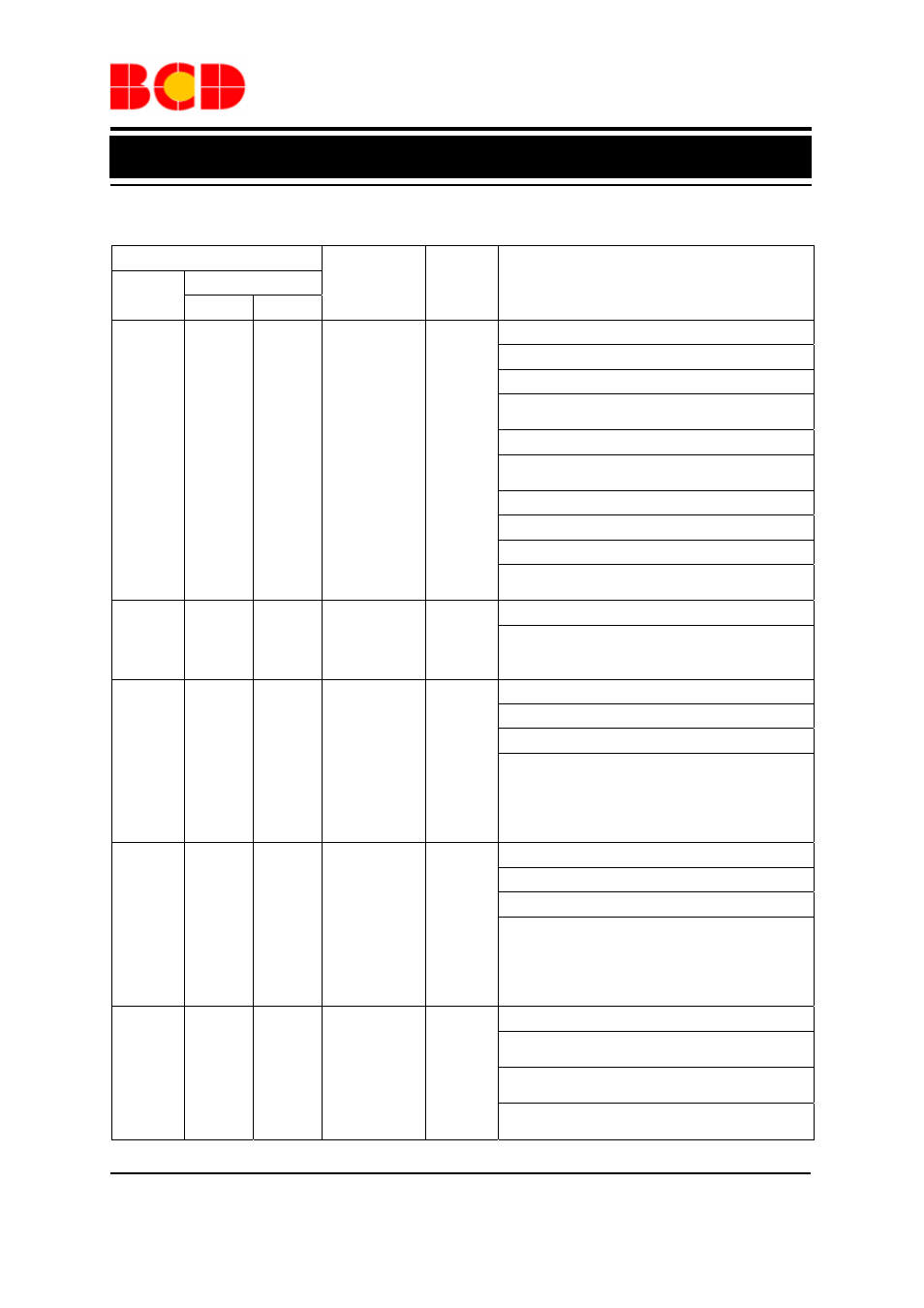
Pin Description
Pin Number
Pin Name
Pin
Type
Pin Function
QFN-56
AP3890
QFN-68
AP3891 AP3892
1 1 1
P1.7/
TXD1/
PINT0.1/
EXTCLKIN/
T0
I/O
Port 1.7 GPIO
8051 P1.7 GPIO
TXD1
This pin also can be configured as TXD of
UART 1
PINT0.1
This pin also can be configured as the
expanded INT0 interrupt
External Clock Input
External clock input source.
T0 Timer 0 Input
This pin also can be configured as Timer 0
input
2 2 2
TESTEN I
Test Mode Enable High Active
This pin has an internal weakly pull low
resistor connected. If it is connected high, the
chip enters into Test Mode condition
3 3 3
P1.2/SDA
(open-drain)
I/O
Port 1.2 GPIO
8051 P1.2 GPIO
SDA
This pin also can be configured as the SDA
signal of the I2C master or I2C slave controller.
In this operation mode, this pin should also be
configured as bi-directional I/O with
open-drain output
4 4 4
P1.3/SCL
(open-drain)
I/O
Port 1.3 GPIO
8051 P1.3 GPIO
SCL
This pin also can be configured as the SCL
signal of the I
2
C master or I
2
C slave controller.
In I
2
C master mode, this pin should be
configured as open-drain output. In I
2
C slave,
this pin should be configured as input only
5 5 5 RSTN I
Reset Low Active
Typically connect a resistor to VDD18 and a
capacitor to VSS
Low asserted and threshold at 0.5×V
DD18
. When
forced low, the chip enters into reset condition
This pin should not be connected to any level
above V
DD18