Preliminary datasheet, Pin description – Diodes AP386X User Manual
Page 4
Preliminary Datasheet
Superior Multi-touch Capacitive Touch Screen Controller AP386X
Aug. 2013 Rev. 1. 0 BCD Semiconductor Manufacturing Limited
4
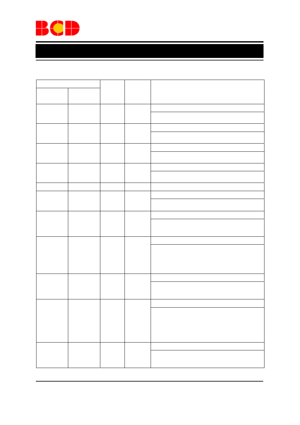
Pin Description
Pin Number
Pin
Name
Pin
Type
Pin Function
QFN-5×5
-
40
AP3860
QFN-6×6
-
48
AP3861
40, 1 to 16
6 to 22
D16 to
D0
I/O, A
Driving Lines 16 to 0
These pins can also be configured as I/O
bi-directional ports for test
-
48, 1 to 5
D22 to
D17
I/O, A
Driving Lines 22 to 17
These pins can also be configured as I/O
bi-directional ports for test
17 23
VDDHV
O
High Voltage. 6V
Charge pump high Voltage. This output pin can be
configured as VDD3V or 6V accordingly
18, 30
24, 35
VDD3V
P
Supply Voltage. 2.8V to 3.6V
A good decoupling capacitor between VDD3V and
VSS pins is critical for good performance
19 25
VSS
P
Ground Voltage. 0V
20 26
VDD18
O
Internal Regulator Output. 1.6V to 2.0V
Typical decoupling capacitors of 0.1
F and 10F
should be connected between VDD18 and VSS
21 27
TESTEN
I
Test Mode Enable High Active
This pin has an internal weakly pull low resistor
connected. If it is connected high, the chip enters into
Test Mode condition
22 28
SS/SCL
I/O
SS/SCL
This pin can be configured as the SCL signal of the
I
2
C master or I
2
C slave controller. When I
2
C is
enabled, the pin is configured as an open-collector.
While in SPI mode, this pin is configured as the
slave chip select pin
23 29
SCK/
GPIO3
I/O
Port 1.3 GPIO
8051 P1.3 GPIO. This pin can also be configured as
the serial clock from SPI master while SPI interface
is activated
24 30
MOSI/
SDA
I/O
SDA
This pin can be configured as the SDA signal of the
I
2
C master or I
2
C slave controller. In this operation
mode, this pin should also be configured as
open-collector. While SPI interface is selected, the
pin serves as the data port from SPI master to SPI
slave
25 31
MISO/
GPIO2
I/O
Port 1.2 GPIO
8051 P1.2 GPIO. This pin can also be configured as
the output data pin from slave to master for SPI
interface