As321, Functional block diagram, Absolute maximum ratings – Diodes AS321 User Manual
Page 3: Recommended operating conditions
AS321
Document number: DS36976 Rev.
2 - 2
3 of 10
February 2014
© Diodes Incorporated
AS321
A Product Line of
Diodes Incorporated
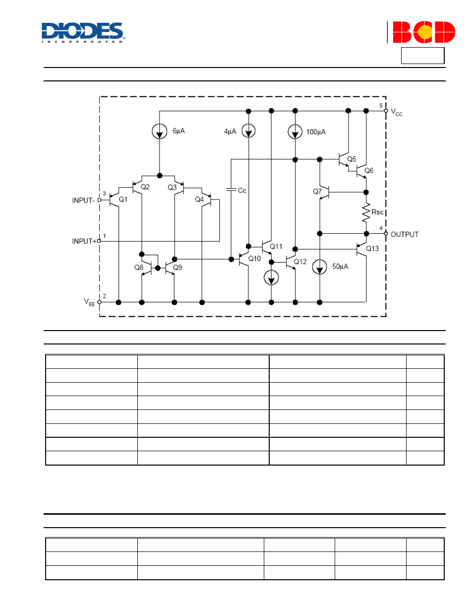
Functional Block Diagram
Absolute Maximum Ratings
(Note 1)
Symbol
Parameter
Rating
Unit
V
S
(V
CC
-V
EE
)
Power Supply Voltage
40
V
V
ID
Differential Input Voltage
40
V
V
IN
Input Voltage
-0.3 to 40
V
θ
JA
Thermal Resistance to Ambient
260
C/W
T
J
Operating Junction Temperature
+150
C
T
STG
Storage Temperature Range
-65 to +150
C
T
LEAD
Lead Temperature (Soldering, 10 Seconds)
+260
C
Note 1:
Stresses greater than those listed under “Absolute Maximum Ratings” may cause permanent damage to the device. These are stress ratings only, and
functional operation of the device at these or any other conditions beyond those indicated under “Recommended Operating Conditions” is not implied.
Exposure to “Absolute Maximum Ratings” for extended periods may affect device reliability.
Recommended Operating Conditions
Symbol
Parameter
Min
Max
Unit
V
CC
Supply Voltage
3
36
V
T
A
Ambient Operating Temperature Range
-40
+85
C