Ap331a, Electrical characteristics, Single differential comparator – Diodes AP331A User Manual
Page 4
AP331A
SINGLE DIFFERENTIAL COMPARATOR
AP331A Rev. 2
4 of 13
FEBRUARY 2009
©
Diodes Incorporated
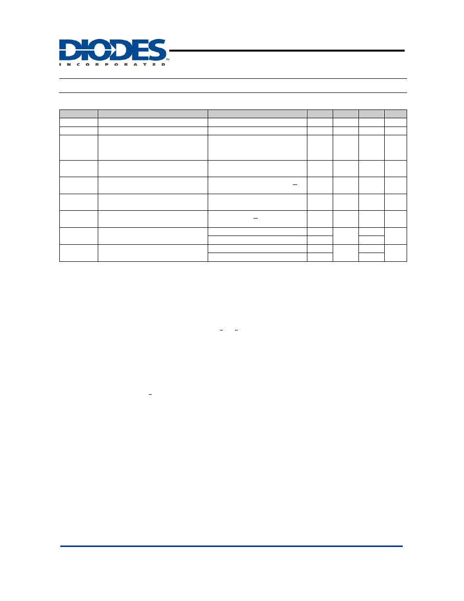
Electrical Characteristics
( V
CC
= 5V ) ( Note 6 )
Symbol
Parameter
Conditions
Min
Typ.
Max
Unit
V
OFFSET
Input Offset Voltage
(Note 11)
- - 9
mV
I
OFFSET
Input Offset Current
I
IN
(+) -I
IN
(-), V
CM
= 0V
-
-
200
nA
I
BIAS
Input Bias Current
I
IN
(+) or I
IN
(-) with Output In
Linear Range, V
CM
= 0V
(Note 7)
- -
500
nA
Input Common Mode Voltage
Range
V
+
=30V (Note 8)
0 -
V
+
-2.0
V
V
SAT
Saturation
Voltage
V
IN
(-) = 1V, V
IN
(+) = 0, I
SINK
<
4mA
- -
700
mV
I
O(Leak)
Output
Leakage
Current
V
IN
(-) = 0, V
IN
(+) = 1V,
V
O
= 30V
- -
1.0
μA
Differential
Input
Voltage
Keep All V
IN
’s > 0V (or V
-
, if
Used), (Note 10)
- - 36
V
θ
JA
Thermal Resistance
Junction-to-Ambient
SOT25 (Note 12)
173
o
C/W
SOT25R (Note 12)
θ
JC
Thermal Resistance
Junction-to-Case
SOT25 (Note 12)
37
o
C/W
SOT25R (Note 12)
Notes: 3. The maximum power dissipation is a function of T
J(MAX)
,
θ
JA
. The maximum allowable power dissipation at any ambient temperature is
P
D
= (T
J(MAX)
-T
A
)/
θ
JA
. All numbers apply for packages soldered directly onto a PC board.
4. Short circuits from the output to V
+
can cause excessive heating and eventual destruction. When considering short circuits to
ground, the maximum output current is approximately 20mA independent of the magnitude of V
+
.
5. This input current will only exist when the voltage at any of the input leads is driven negative. It is due to the collector-base
junction of the input PNP transistors becoming forward biased and thereby acting as input diode clamps. In addition to this
diode action, there is also lateral NPN parasitic transistor action on the IC chip. This transistor action can cause the output
voltages of the comparators to go to the V
+
voltage level (or to ground for a large overdrive) for the time duration that an input
is driven negative. This is not destructive and normal output states will re-establish when the input voltage, which is negative,
again returns to a value greater than -0.3V.
6. The AP331A temperature specifications are limited to 0°C < T
OP
< +70°C.
7. The direction of the input current is out of the IC due to the PNP input stage. This current is essentially constant, independent
of the state of the output so no loading change exists on the reference or input lines.
8. The input common-mode voltage or either input signal voltage should not be allowed to go negative by more than 0.3V. The
upper end of the common-mode voltage range is V
+
-1.5V at 25°C, but either or both inputs can go to 36V without damage,
independent of the magnitude of V
+
.
9. The response time specified is for a 100mV input step with 5mV overdrive. For larger overdrive signals 300ns can be
obtained, see typical performance characteristics section.
10. Positive excursions of input voltage may exceed the power supply level. As long as the other voltage remains within the
common-mode range, the comparator will provide a proper output state. The low input voltage state must not be less than
-0.3V (or 0.3V below the magnitude of the negative power supply, if used).
11. At output switch point, V
O
~ 1.4V, R
S
=0
Ω with V
+
from 5V to 30V; and over the full input common-mode range (0V to V
+
-1.5V),
at 25°C.
12. Test condition for SOT25 and sot25R: Device mounted on FR-4 substrate PC board, 2oz copper, with minimum recommended pad layout.