New prod uc t ah1902, Pin descriptions, Functional block diagram – Diodes AH1902 User Manual
Page 2
AH1902
Document number: DS36533 Rev. 2 - 2
2 of 10
January 2014
© Diodes Incorporated
NEW PROD
UC
T
AH1902
Pin Descriptions
Package: X1-DFN1216-4
Pin Number
Pin Name
Function
1
OUTPUT Output
Pin
2 GND
Ground
Pin
3 NC
No Connection (Note 5)
4 V
DD
Power Supply Input
Pad Pad
The center exposed pad - It is internally connected to V
DD
pin and should not
be connected to GND or any other signal on the PCB. The exposed pad
should be left open (unconnected) on the PCB layout.
Package: X2-DFN2015-6
Pin Number
Pin Name
Function
1 OUTPUT
Output
Pin
2 NC
No Connection (Note 5)
3 NC
No Connection (Note 5)
4 GND
Ground
Pin
5 NC
No Connection (Note 5)
6 V
DD
Power Supply Input
Pad Pad
The center exposed pad – No connection internally.
The exposed pad can be left open (unconnected) or tied to the GND on the
PCB layout.
Note:
5. NC is “No Connection” pin and is not connected internally. This pin can be left open or tied to ground.
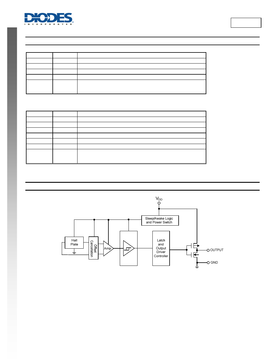
Functional Block Diagram