Absolute maximum ratings, Recommended operating conditions, Electrical characteristics – Diodes AH180N User Manual
Page 3: Ah180n
AH180N
Document number: DS32174 Rev. 4 - 2
3 of 8
August 2012
© Diodes Incorporated
AH180N
Absolute Maximum Ratings
(Note 4) (@T
A
= +25°C, unless otherwise specified.)
Symbol Parameter
Ratings
Unit
V
DD
Supply Voltage (Note 5)
7
V
B
Magnetic Flux Density
Unlimited
P
D
Package
Power
Dissipation
SC59 230
mW
TSOT23 230
SOT553 230
Ts
Storage Temperature Range
-65 to +150
°C
T
J
Maximum Junction Temperature
150
°C
Notes:
4. Stresses greater than the 'Absolute Maximum Ratings' specified above, may cause permanent damage to the device. These are stress ratings
only; functional operation of the device at these or any other conditions exceeding those indicated in this specification is not implied. Device
reliability may be affected by exposure to absolute maximum rating conditions for extended periods of time
5. The absolute maximum V
DD
of 7V is a transient stress rating and is not meant as a functional operating condition. It is not recommended to
operate the device at the absolute maximum rated conditions for any period of time.
Recommended Operating Conditions
(@T
A
= +25°C, unless otherwise specified.)
Symbol Parameter Conditions
Rating
Unit
V
DD
Supply Voltage
Operating
2.5 to 5.5
V
T
A
Operating Temperature Range
Operating
-40 to +85
°C
Electrical Characteristics
(@T
A
= +25°C, V
DD
= 3V, unless otherwise specified.)
Symbol Parameter
Conditions
Min
Typ
Max
Unit
V
OUT
Output
On
Voltage
I
OUT
= 1mA
⎯
0.1 0.3 V
Ioff Output
Leakage
Current V
OUT
= 5.5V, Output Off
⎯
<0.1 1 µA
Idd(en)
Supply Current
Chip Enable, T
A
= +25°C, V
DD
= 3V
⎯
3 6
mA
Idd(en)
Chip Enable, T
A
= -40 to +85°C,
V
DD
= 2.5V to 5.5V
⎯
3 12
mA
Idd(dis)
Chip Disable, T
A
= +25
°C, V
DD
= 3V
⎯
5 10 µA
Idd(dis)
Chip Disable, T
A
= -40 to 85
°C,
V
DD
= 2.5V to 5.5V
⎯
5 28 µA
Idd(avg)
Average Supply Current,
T
A
= +25
°C, V
DD
= 3V
⎯
8 16 µA
Idd(avg)
Average Supply Current,
T
A
= -40 to +85
°C, V
DD
= 2.5V to 5.5V
⎯
8 40 µA
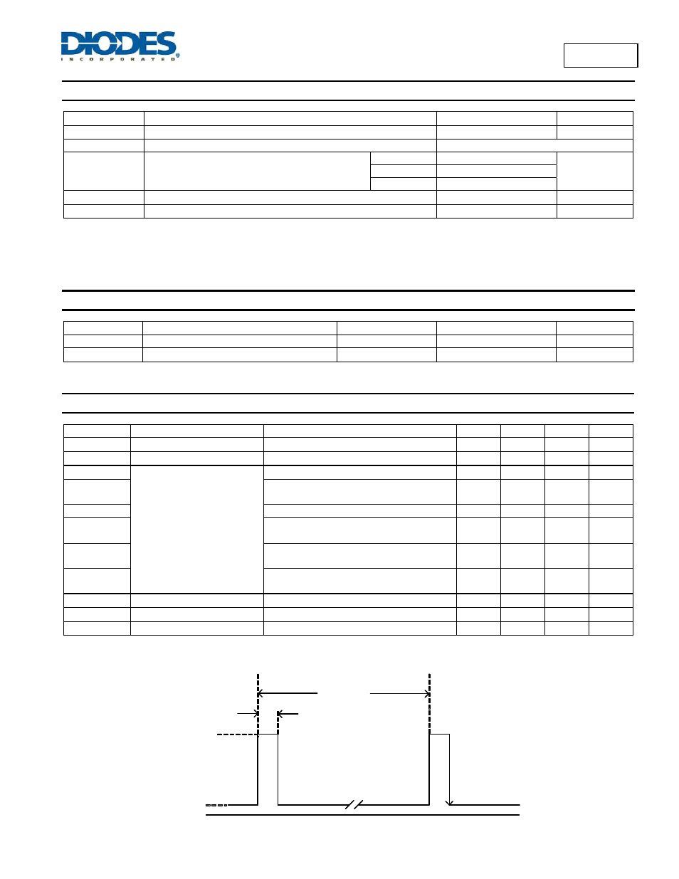
Tawake Awake
Time
(Note
6)
⎯
75 125 µs
Tperiod Period
(Note
6)
⎯
75 125 ms
D.C. Duty
Cycle
⎯
0.1
⎯
%
Notes:
6. When power is initially turned on, V
DD
must be within its correct operating range (2.5V to 5.5V) to guaranteed the output sampling.
The output state is valid after the second operating cycle (typical 150ms).
Idd (dis)
Idd(en)
Tawake
Tperiod
0
Sample and output
latched