New prod uc t ah1903, Pin descriptions, Functional block diagram – Diodes AH1903 User Manual
Page 2: Absolute maximum ratings
AH1903
Document number: DS36568 Rev. 2 - 2
2 of 12
January 2014
© Diodes Incorporated
NEW PROD
UC
T
AH1903
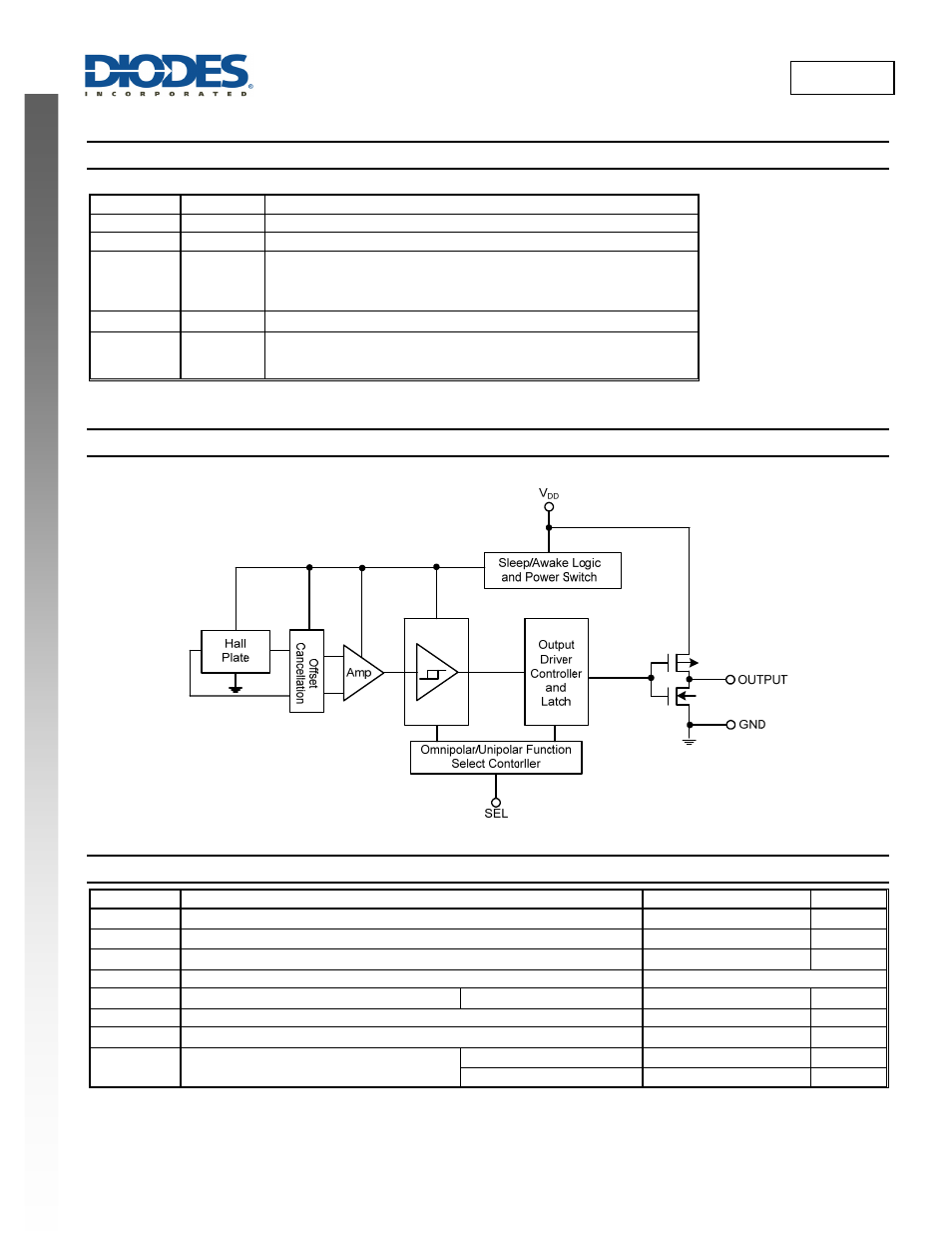
Pin Descriptions
Package: X1-DFN1216-4
Pin Number
Pin Name
Function
1
OUTPUT Output
Pin
2 GND
Ground
Pin
3 SEL
Unipolar or Omnipolar Operation Select Pin;
For Unipolar operation, pull-up the SEL pin to V
DD
or leave it unconnected.
The SEL pin is internally pulled high.
For Omnipolar operation, connect the SEL pin to GND.
4
V
DD
Power Supply Input
Pad Pad
The center exposed pad - It is internally connected to V
DD
pin and should
not be connected to GND or any other signal on the PCB. The exposed pad
should be left open (unconnected) on the PCB layout.
Functional Block Diagram
Absolute Maximum Ratings
(Note 5) (@T
A
= +25°C, unless otherwise specified.)
Symbol Parameter
Rating
Unit
V
DD
Supply Voltage (Note 6)
6 V
V
DD_REV
Reverse Supply Voltage
-0.3
V
I
OUTPUT
Output current (source and sink)
3
mA
B
Magnetic Flux Density
Unlimited
P
D
Package Power Dissipation
X1-DFN1216-4
230
mW
Ts
Storage Temperature Range
-65 to +150
°C
T
J
Maximum Junction Temperature
150
°C
ESD HBM
Human Body Model (HMB) ESD capability
V
DD
, GND and OUTPUT pins
8 kV
Logic SEL pin
6
kV
Notes:
5. Stresses greater than the 'Absolute Maximum Ratings' specified above may cause permanent damage to the device. These are stress ratings only;
functional operation of the device at these or any other conditions exceeding those indicated in this specification is not implied. Device reliability may be
affected by exposure to absolute maximum rating conditions for extended periods of time.
6. The absolute maximum V
DD
of 6V is a transient stress rating and is not meant as a functional operating condition. It is not recommended to
operate the device at the absolute maximum rated conditions for any period of time.