Preliminary datasheet, Pin description – Diodes AP3612 User Manual
Page 3
Preliminary Datasheet
Boost Type LED Driver with 12-Channel Current Source AP3612
Aug. 2012 Rev. 1. 1 BCD Semiconductor Manufacturing Limited
3
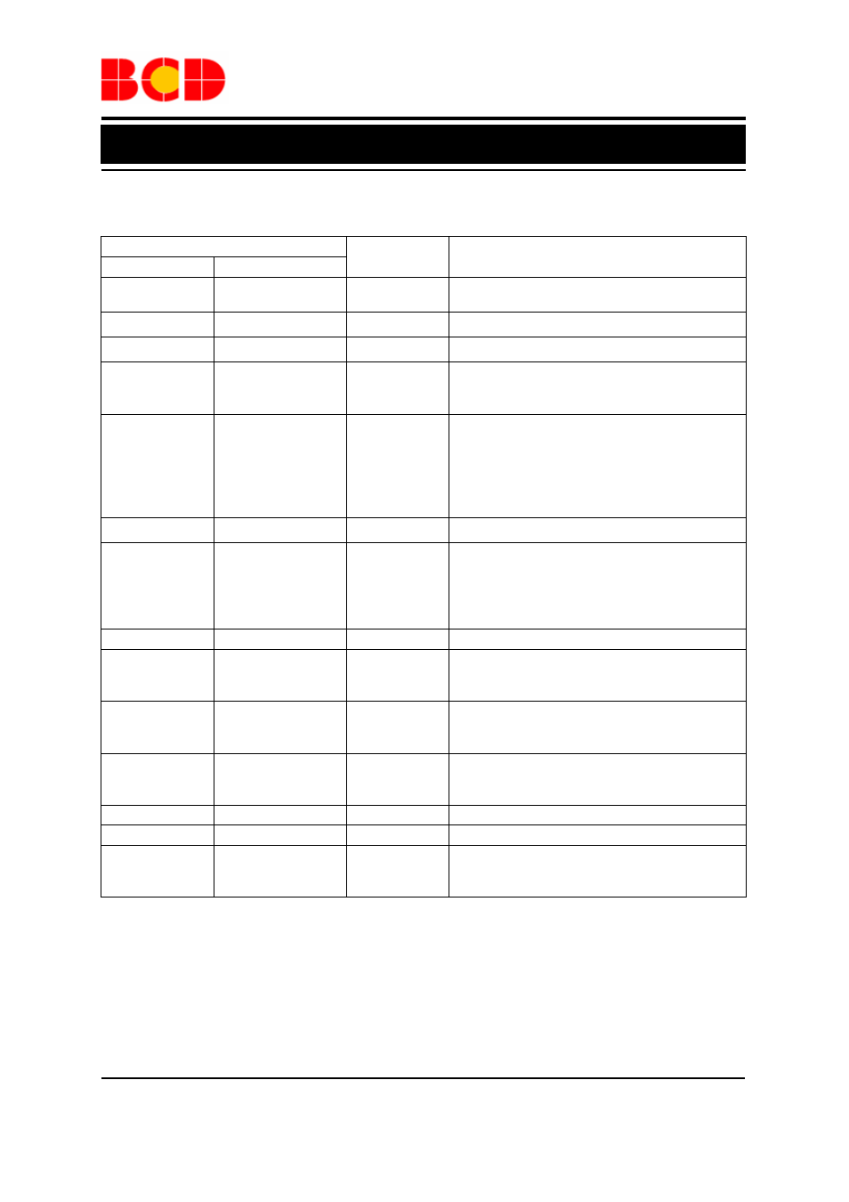
Pin Description
Pin Number
Pin Name
Function
HSOP-28 SOIC-24
28,1,2,3,4,5,
8,9,10,11,12 ,14
18,19,20,21, 22,23,
1, 2, 3, 4, 5, 7
CH1 to CH12
LED current sink. Leave the pin open directly
if not used
6, 21,25
NC
No connection
7, 20
24
GND
Ground pin
13
6
ISET
LED current setting pin. The corresponding
maximum current of all strings is set through
connecting a resistor from this pin to GND
15
8 OVP
Over voltage protection pin. When the OVP
pin voltage exceeds 2.0V, the OVP is triggered
and the power switch is turned off. When the
OVP pin voltage drops below hysteresis
voltage, the OVP is released and the power
switch will resume normal operation
16
9
RT
Frequency control pin
17 10 EN
ON/OFF control pin. Forcing this pin above
2.4V enables the IC while below 0.5V shuts
down the IC. When the IC is in shutdown
mode, all functions are disabled to decrease
the supply current below 3
µA
18 11 CS
Power switch current sense input
19 12
OUT
Boost converter power switch gate output.
This pin output high voltage (5V/V
IN
-0.5V) to
drive the external N-MOSFET
22 13
VCC
5V linear regulator output pin. This pin should
be bypassed to GND (recommend to connect
with GND pin) with a ceramic capacitor
23 14
VIN
Supply input pin. A capacitor (typical 10
µF)
should be connected between the VIN and
GND to keep the DC input voltage constant
24 15
STATUS
LED operation status output
26 16
COMP
Soft-start and control loop compensation
27 17
DIM
PWM dimming control pin. Adding a PWM
signal to this pin to control LED dimming. If
not used, connect it to the high level