Data sheet – Diodes AP3605 User Manual
Page 4
4
Jan. 2013 Rev. 1. 8
BCD Semiconductor Manufacturing Limited
4-Channel Charge Pump LED Driver with Current Balancing and Wide Range PWM Dimming AP3605
Data Sheet
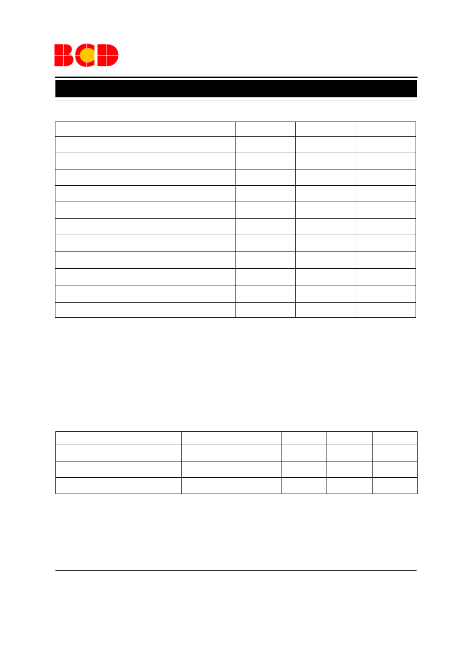
Note 2: Stresses greater than those listed under "Absolute Maximum Ratings" may cause permanent damage to
the device. These are stress ratings only, and functional operation of the device at these or any other conditions
beyond those indicated under "Recommended Operating Conditions" is not implied. Exposure to "Absolute Max-
imum Ratings" for extended periods may affect device reliability.
Parameter
Symbol
Min
Max
Unit
Input Voltage
V
IN
2.7
5.5
V
Operating Temperature
T
A
-40
85
o
C
Current Source Set Resistor
R
ISET
1.44
k
Ω
Recommended Operating Conditions
Absolute Maximum Ratings (Note 2)
Parameter
Symbol
Value
Unit
Input Voltage
V
IN
-0.3 to 6
V
EN Pin Voltage
V
EN
-0.3 to 6
V
V
OUT1
Pin Voltage
V
OUT1
-0.3 to 6
V
V
OUT2
Pin Voltage
V
OUT2
-0.3 to 6
V
ISET Pin Voltage
V
ISET
-0.3 to 6
V
Output Current at V
OUT2
Pin
I
OUT2
150
mA
Thermal Resistance (Junction to Ambient, no Heat sink)
R
θJA
60
o
C/W
Operating Junction Temperature
T
J
150
o
C
Storage Temperature Range
T
STG
-65 to 150
o
C
Lead Temperature (Soldering, 10sec)
T
LEAD
260
o
C
ESD (Human Body Model)
2000
V